Organic Light-Emitting Diode Pixel Circuit, Drive Method Thereof, and Display Device

a light-emitting diode and circuit technology, applied in semiconductor devices, instruments, computing, etc., can solve the problems of affecting the display quality of the display screen, unfavorable improvement of production yield and production efficiency, and complicated control circuit and manufacturing process, etc., to achieve simple timing, easy-to-implement circuit, and less control signals

Active Publication Date: 2015-02-05
BOE TECH GRP CO LTD +1
View PDF4 Cites 17 Cited by
  • Summary
  • Abstract
  • Description
  • Claims
  • Application Information

AI Technical Summary

Benefits of technology

[0005]Objects to be achieved by the present invention are to provide an OLED pixel circuit whose control circuit and manufacturing process are relatively simple, a drive method thereof and a display device, aiming at the above problem in the prior art that the control circuit and manufacturing process of an in-cell touch screen are relatively complicated, which is unfavorable for improving production yield and production efficiency.
[0031]The OLED pixel circuit of the present invention comprises the photodiode, which renders the display screen capable of directly sensing a signal generated by a touch, such that the control circuit of the pixel and the manufacturing process are simplified, this further improves production efficiency and production yield, and most importantly, helps to reduce cost. Meanwhile, the OLED pixel circuit can compensate non-uniformity of the threshold voltage of a TFT, thus improving picture uniformity of the organic light emitting display. In addition, two layers of indium tin oxide films are omitted in production process, and therefore light transmittance can be effectively improved, thus improving display quality of the display screen.
[0033]The display device of the present invention includes the above OLED pixel circuit, and accordingly, it is thinner in overall thickness, lighter in weight, and lower in production cost. By providing the above circuit in each sub-pixel, sensitivity of the display screen to a touch may be significantly improved, furthermore, the photodiode works by sensing the change of light, and therefore, floating touch can be achieved on the display screen.
[0044]The drive method of the OLED pixel circuit of the present invention has less control signals, simple timing, and an easy-to-implement circuit, and is convenient and practical.

Problems solved by technology

The inventors found that at least the following problems exist in the prior art: for an in-cell touch screen, as the function of sensing signals by the touchpad is embedded in the pixel circuit, its control circuit and manufacturing process are relatively complicated, which is unfavorable for improving production yield and production efficiency.
In addition, for the in-cell touch screen, its pixel aperture ratio may be decreased, which further results in degraded display quality of display screen.

Method used


Image

  • Organic Light-Emitting Diode Pixel Circuit, Drive Method Thereof, and Display Device
  • Organic Light-Emitting Diode Pixel Circuit, Drive Method Thereof, and Display Device
  • Organic Light-Emitting Diode Pixel Circuit, Drive Method Thereof, and Display Device

Examples


embodiment 1

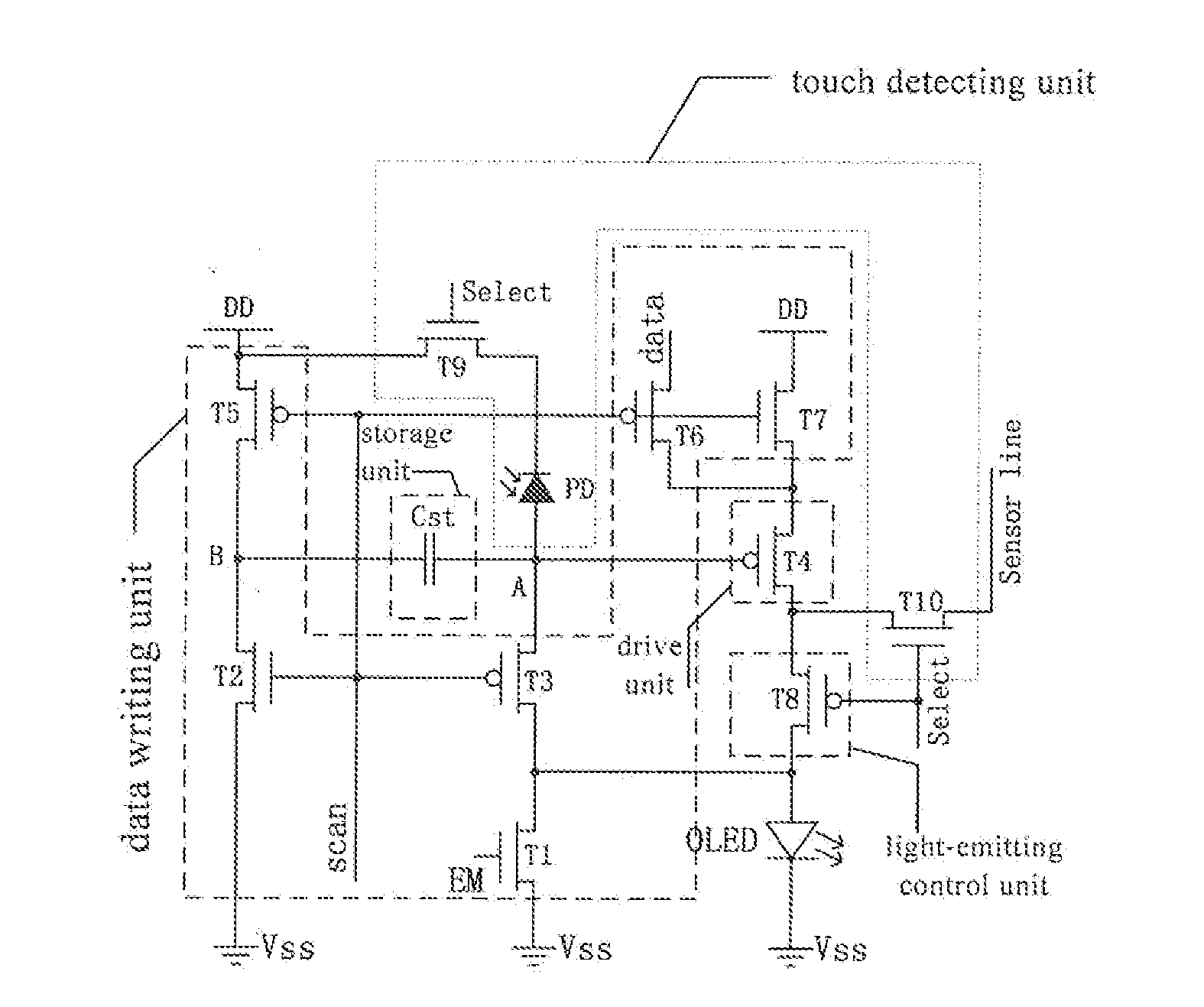
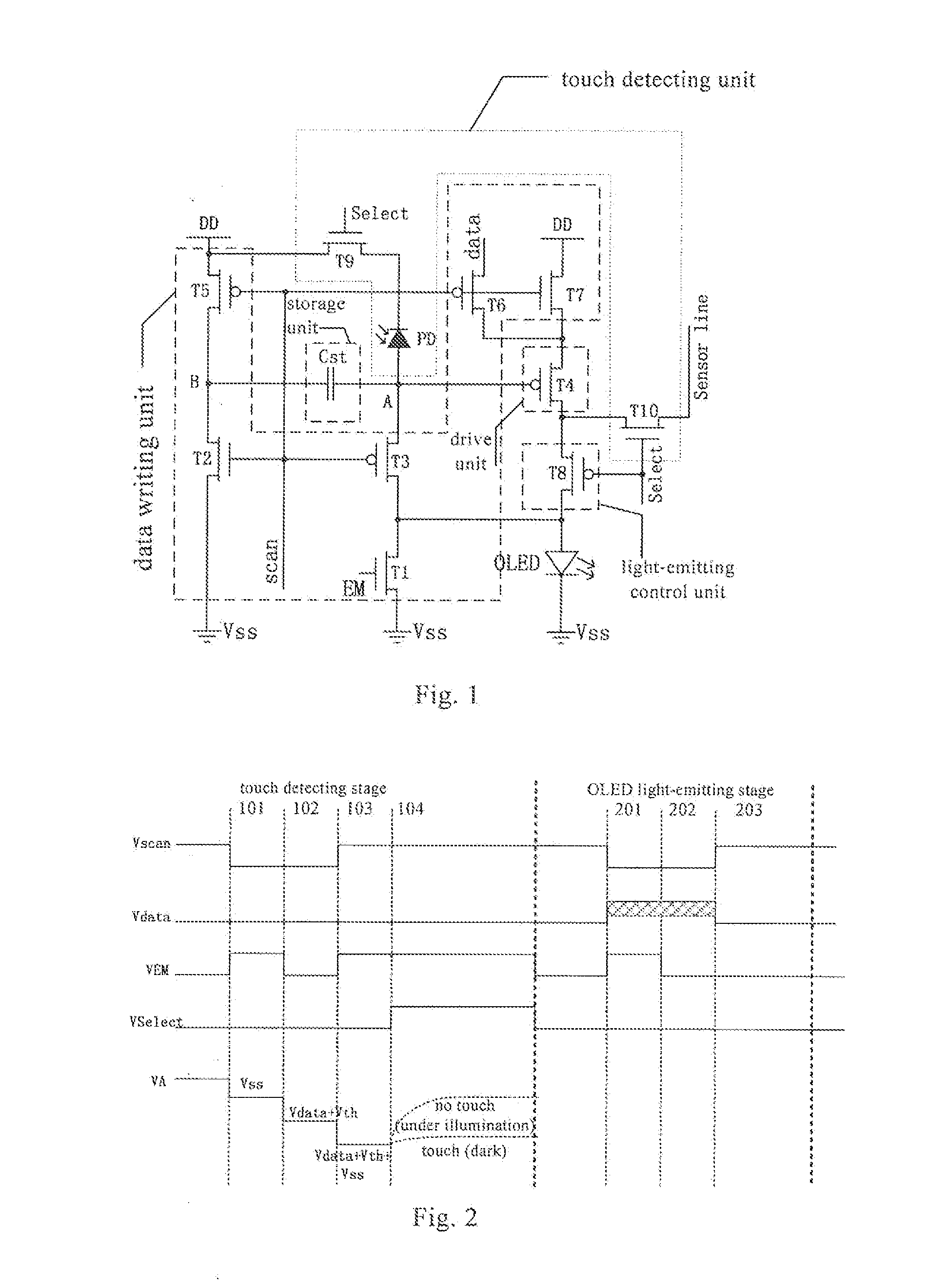
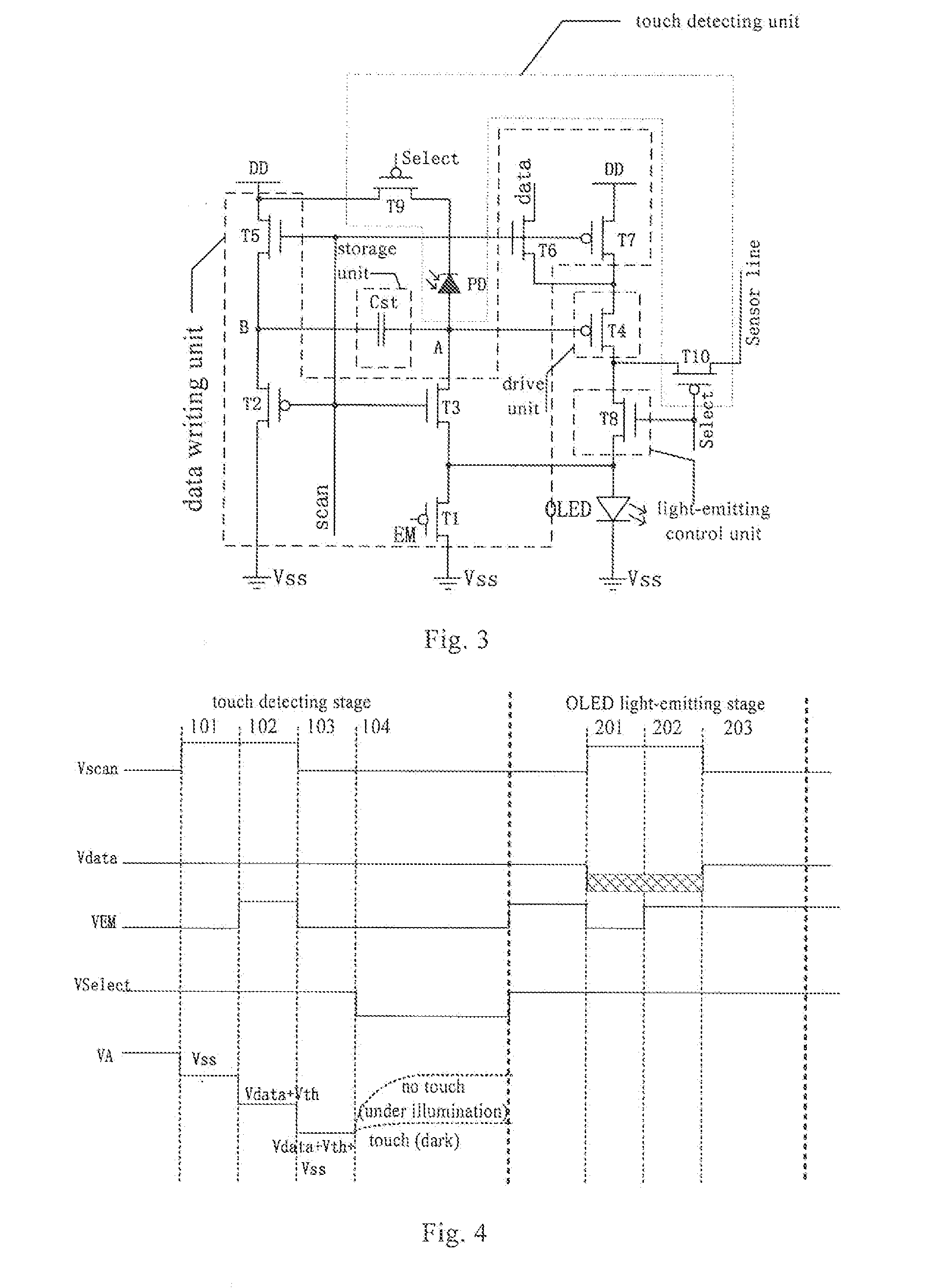
[0056]This embodiment provides an OLED pixel circuit, and as shown in FIG. 1, the OLED pixel circuit comprises:

[0057]a data writing unit, a storage unit, a drive unit, an organic light-emitting diode OLED, a light-emitting control unit and a touch detecting unit; wherein,

[0058]the data writing unit, in a touch detecting stage and an OLED light-emitting stage, is used for writing a power supply voltage signal into the storage unit under the control of a light-emitting control line and a scanning line, and writing a data line voltage signal into the storage unit under the control of the scanning line;

[0059]the storage unit is used for supplying voltage to the drive unit;

[0060]the touch detecting unit, in the touch detecting stage, is used for sensing touch under the control of a touch signal level control line, and generating a detecting signal;

[0061]the drive unit, in the touch detecting stage, is used for converting the detecting signal into a touch output signal, which is output vi...

embodiment 2

[0102]This embodiment provides a display device, which comprises the above-described OLED pixel circuit, and other known structures such as a substrate. The display device may be an OLED display device or a product or component with display function, which uses OLED display technique, such as a mobile phone, a tablet computer, a television, a display, a notebook computer, a digital frame or a navigator.

[0103]The display device of this embodiment comprises the above-described OLED pixel circuit, and therefore, it is thinner in overall thickness, lighter in weight, and lower in production cost. By providing the above circuit in each sub-pixel, sensitivity of the display screen to a touch may be significantly improved, furthermore, the photodiode works by sensing changes of light, and therefore, floating touch can be achieved on the display screen.


PUM


Abstract

The present invention belongs to the field of display technology, and provides an OLED pixel circuit, a drive method thereof and a display device, which may solve the problem of relatively complicated control circuit and manufacturing process of an existing in-cell touch screen. In the OLED pixel circuit of the present invention, the data writing unit is for writing power supply voltage signal and data line voltage signal into the storage unit; the storage unit is for supplying voltage to the drive unit; the touch detecting unit is for sensing touch and generating a detecting signal; the drive unit is for converting the detecting signal into a touch output signal and for 10 providing drive current fin the OLED; and the light-emitting control unit is for turning on the drive unit and the OLED. The present invention may allow the touch display device to be thinner and lighter.

Description

FIELD OF THE INVENTION[0001]The present invention relates to the field of touch display technology, and particularly, to an organic light-emitting diode (OLED) pixel circuit, a drive method thereof, and a display device.DESCRIPTION OF THE RELATED ART[0002]Touch screen, as one of the simplest, most convenient, and most natural human-machine interaction devices, has been widely applied in various electronic devices, such as mobile phones, notebook computers, digital cameras and the like. Touch screens, according to the way they are mounted, may be classified into two types, namely, external touch screens and in-cell touch screens. An external touch screen is formed by arranging a touch device, which generally includes a touchpad and a protection layer e.g. gorilla glass), on a display panel, the touchpad is disposed on the display panel, and the touch screen operates based on the change in light or pressure sensed by the touchpad.[0003]In in-cell touch screen technique, the function o...

Claims


Application Information

Patent Timeline
Patent Type & Authority Applications(United States)
IPC IPC(8): G09G3/32G06F3/044H01L27/32
CPCG09G3/3266H01L27/323G06F3/044H01L27/3262H01L27/3265H01L27/3227G09G3/3233G09G2300/0819G09G2300/0842G09G2300/0861G09G2320/0295G09G2320/043G09G2360/148G06F3/0412G06F3/042G06F3/04184G06F3/041G06F3/04166
Inventor ZHOU, QUANGUOQI, XIAOJING
Owner BOE TECH GRP CO LTD
Why Eureka
Try Eureka