Measurement method of overlay mark
a measurement method and overlay mark technology, applied in the field of integrated circuit (ic) fabrication, can solve problems such as difficulty in proving overlay measurement, and achieve the effect of reliable and accurate overlay data
- Summary
- Abstract
- Description
- Claims
- Application Information
AI Technical Summary
Benefits of technology
Problems solved by technology
Method used
Image

Examples
first embodiment
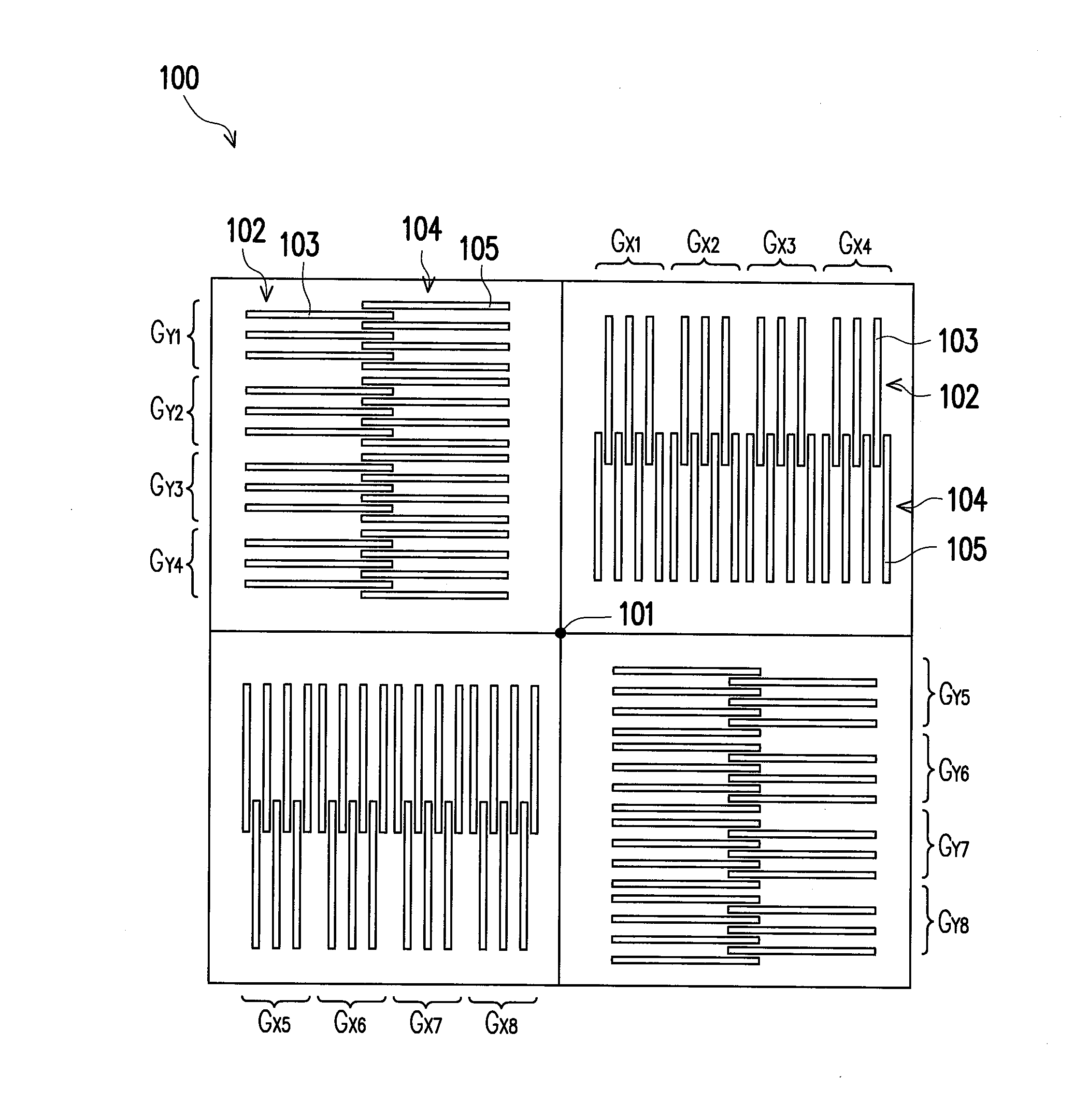
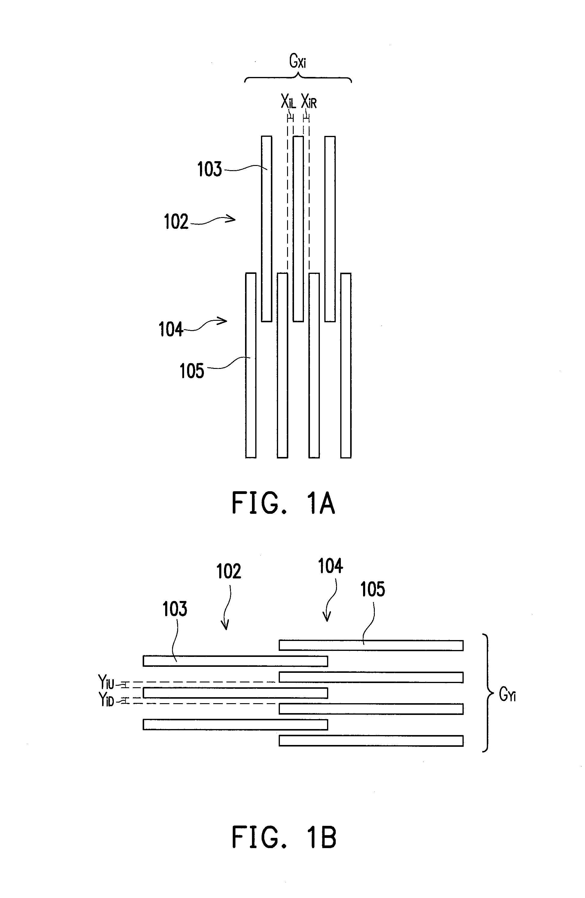
[0042]FIG. 1 illustrates a schematic top view of an overlay mark according to a first embodiment of the present invention.
[0043]Referring to FIG. 1, the overlay mark 100 of the invention includes a plurality of patterns 103 of a previous layer 102 and a plurality of patterns 105 of a current layer 104. The patterns 103 of the previous layer 102 are substantially arranged symmetrical with respect to a central point 101, and the second patterns 105 of the current layer 104 are substantially arranged symmetrical with respect to the central point 101. By such substantially symmetrical design, the overlay mark 100 can be used to measure the alignment accuracy between layers with an optical measurement tool. The optical tool can be a KLA optical measurement tool.
[0044]Besides, the patterns 103 of the previous layer 102 and the patterns 105 of the current layer 104 are divided into, for example but not limited to, sixteen groups GX1, GX2, . . . , GX8 and GY1, GY1, . . . , GY1, as shown in ...
second embodiment
[0058]FIG. 2 illustrates a schematic top view of an overlay mark according to a second embodiment of the present invention.
[0059]The overlay mark 200 of the invention includes a plurality of patterns 203 of a previous layer 202 and a plurality of patterns 205 of a current layer 204. The patterns 203 of the previous layer 202 are substantially arranged symmetrical with respect to a central point 201, and the second patterns 205 of the current layer 204 are substantially arranged symmetrical with respect to the central point 201. By such substantially symmetrical design, the overlay mark 200 can be used to measure the alignment accuracy between layers with an optical measurement tool, such as a KLA optical measurement tool.
[0060]Besides, the patterns 203 of the previous layer 202 and the patterns 205 of the current layer 204 are divided into, for example but not limited to, sixteen groups GX1, GX2, . . . , GX8 and GY1, GY1, . . . , GY1, as shown in FIG. 2. The groups GX1, GX2, . . . ,...
third embodiment
[0072]FIG. 3 illustrates a schematic top view of an overlay mark according to a third embodiment of the present invention.
[0073]The overlay mark 300 of the invention includes a plurality of patterns 303 of a previous layer 302 and a plurality of patterns 305 of a current layer 304. The patterns 303 of the previous layer 302 are substantially arranged symmetrical with respect to a central point 301, and the second patterns 305 of the current layer 304 are substantially arranged symmetrical with respect to the central point 301. By such substantially symmetrical design, the overlay mark 300 can be used to measure the alignment accuracy between layers with an optical measurement tool, such as a KLA optical measurement tool.
[0074]Besides, the patterns 303 of the previous layer 302 and the patterns 305 of the current layer 204 are divided into, for example but not limited to, sixteen groups GX1, GX2, . . . , GX8 and GY1, GY1, . . . , GY1, as shown in FIG. 3. The groups GX1, GX2, . . . , ...
PUM
| Property | Measurement | Unit |
|---|---|---|
| wavelength | aaaaa | aaaaa |
| wavelength regions | aaaaa | aaaaa |
| wavelength | aaaaa | aaaaa |
Abstract
Description
Claims
Application Information
 - R&D
- Intellectual Property
- Life Sciences
- Materials
- Tech Scout
- Unparalleled Data Quality
- Higher Quality Content
- 60% Fewer Hallucinations
Browse by: Latest US Patents, China's latest patents, Technical Efficacy Thesaurus, Application Domain, Technology Topic, Popular Technical Reports.
© 2025 PatSnap. All rights reserved.Legal|Privacy policy|Modern Slavery Act Transparency Statement|Sitemap|About US| Contact US: help@patsnap.com