Pixel structure

a pixel structure and panel technology, applied in non-linear optics, instruments, optics, etc., can solve the problems of reducing the transmittance of the lcd panel, and achieve the effects of satisfactory display quality, favorable transmittance, and sufficient transmittan

Active Publication Date: 2015-03-12
AU OPTRONICS CORP
View PDF3 Cites 16 Cited by
  • Summary
  • Abstract
  • Description
  • Claims
  • Application Information

AI Technical Summary

Benefits of technology

[0009]As discussed above, in the pixel structure described herein, the conventional issue that the liquid crystal molecules above pixel electrodes are tilted in a direction different from that of the liquid crystal molecules above alignment slits does not arise. That is, in the pixel structure described herein, the liquid crystal molecules above the pixel electrodes and the liquid crystal molecules above the alignment slits are tilted in the same direction, such that the pixel structure provided herein may have favorable transmittance without triggering the issue of disclination lines or disclination nodes. As such, the resultant LCD panel may have sufficient transmittance and satisfactory display quality.

Problems solved by technology

In a conventional FFS LCD panel, however, electric field sensed by liquid crystal molecules above pixel electrodes is different from electric field sensed by liquid crystal molecules above alignment slits among branch portions of the pixel electrodes, such that said liquid crystal molecules at different locations may be tilted in different directions, which may lead to unexpected disclination lines or disclination nodes and further reduce transmittance of the LCD panel.

Method used


Image

  • Pixel structure
  • Pixel structure
  • Pixel structure

Examples


first embodiment

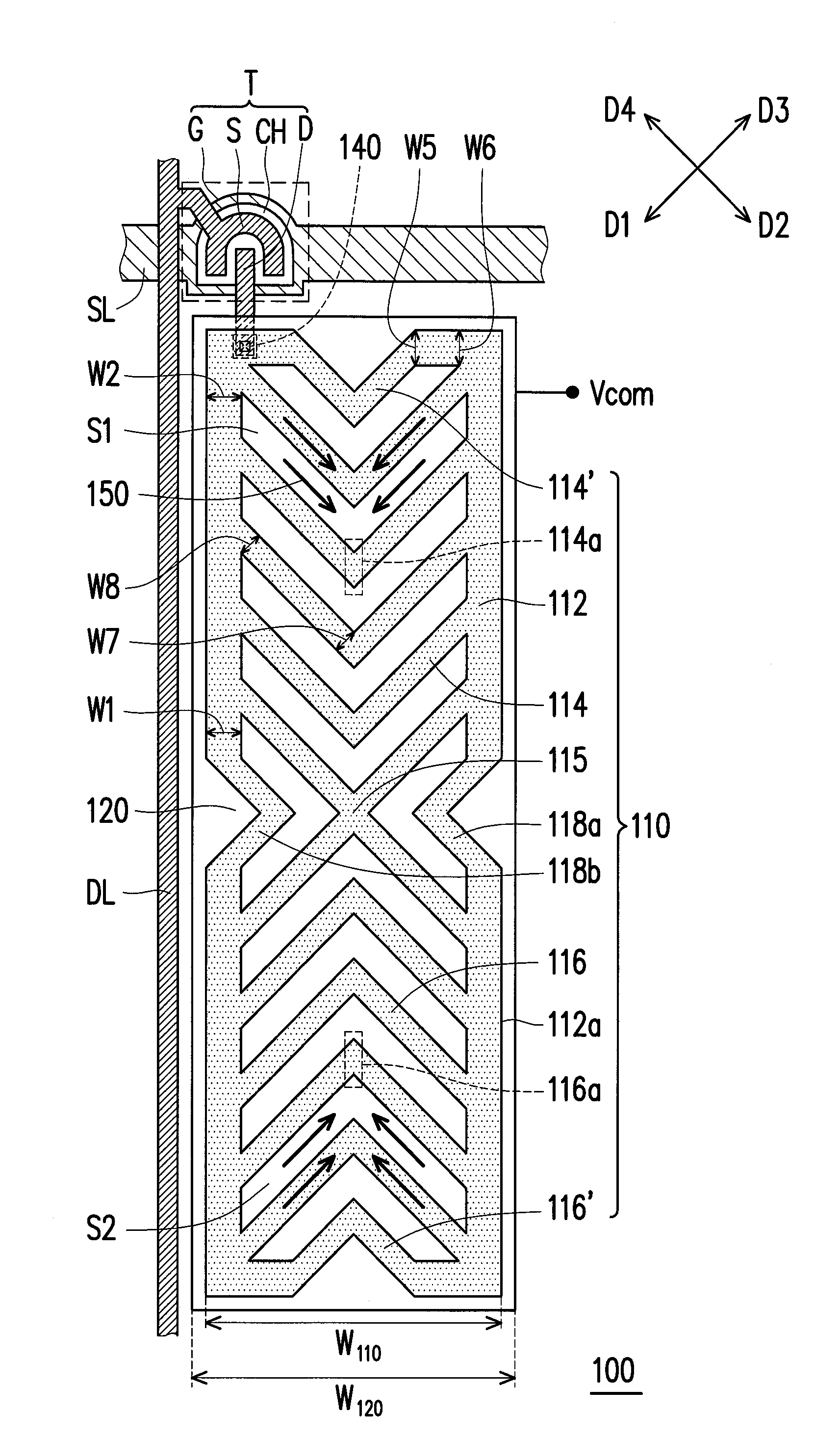
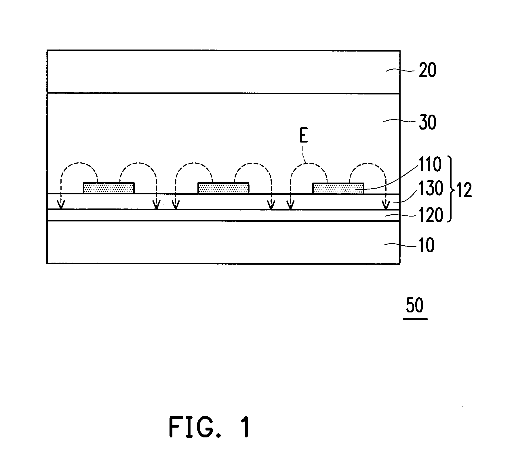
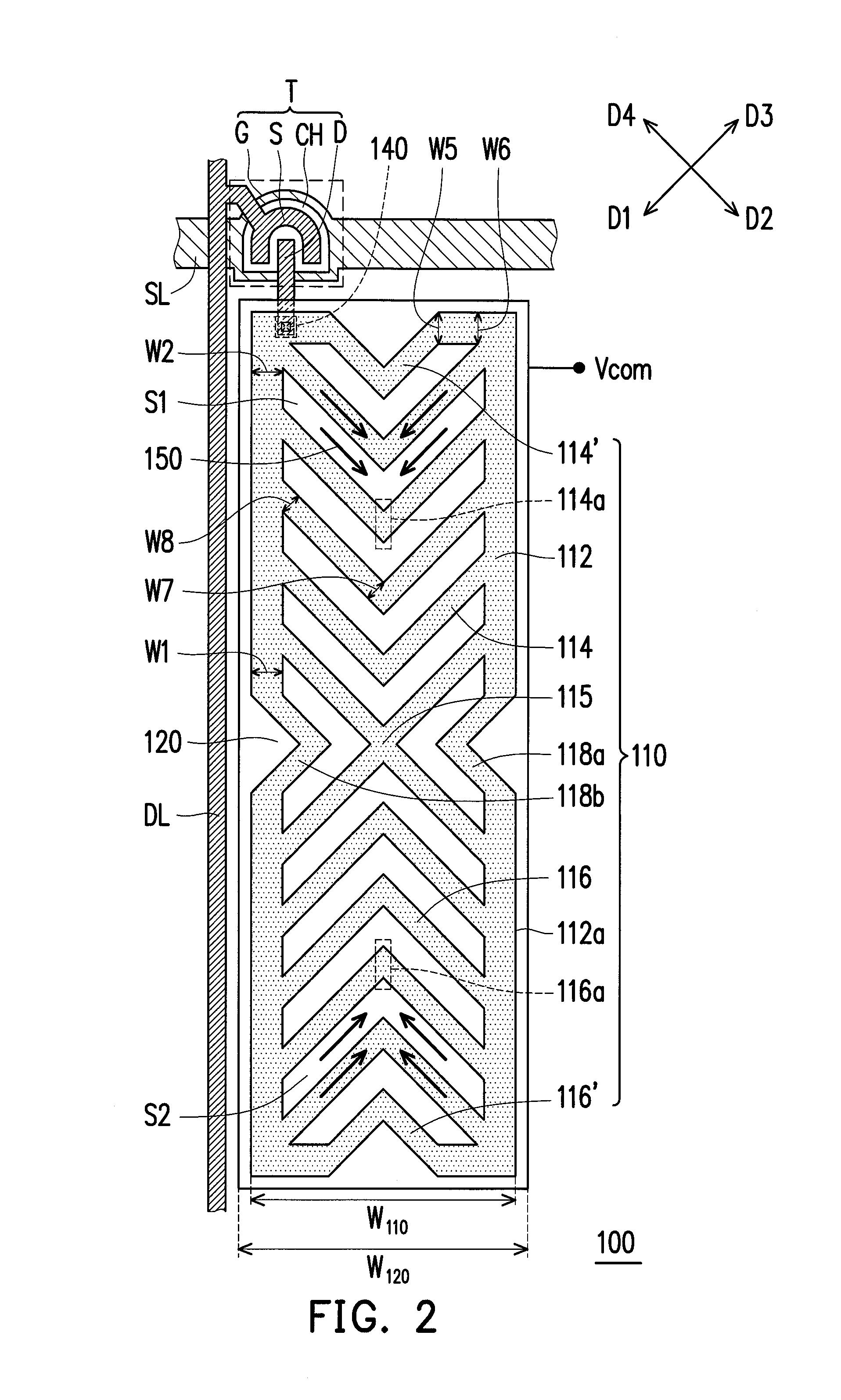
[0023]FIG. 1 is a schematic cross-sectional view illustrating an LCD panel 50 according to an embodiment of the invention. FIG. 2 is a schematic top view illustrating a pixel structure 100 according to the invention. For illustrative purposes, FIG. 2 merely shows one pixel structure 100 in a pixel array layer 12 of the LCD panel 50 in FIG. 1, and people skilled in the art should be able to understand that the pixel array layer 12 depicted in FIG. 1 is constituted by plural pixel structures 100 (shown in FIG. 2) arranged in arrays. Besides, FIG. 1 merely illustrates several components of the pixel structure 100, and the scan line SL, the data line DL, and the active device T are not shown in FIG. 1. The detailed structure and components of the pixel structure 100 are provided in FIG. 2.

[0024]The LCD panel 50 is a vertical alignment-fringe field switching (VA-FFS) LCD panel, for instance, and the VA-FFS LCD panel is characterized by both high contrast ratio (i.e., the feature of the v...

second embodiment

[0044]FIG. 3 is a schematic top view illustrating a pixel structure 200 according to the invention. The embodiment depicted in FIG. 3 is similar to that depicted in FIG. 2; therefore, the identical or similar devices in these two embodiments are represented by the identical or similar reference numbers and will not be further explained. The difference between the embodiment depicted in FIG. 3 and the embodiment depicted in FIG. 2 lies in that the outer edge of the enclosed-frame-shaped portion is shaped in a different manner according to the present embodiment. To be specific, in FIG. 3, the enclosed-frame-shaped portion 212 of the first electrode layer 210 has a step-wise outer edge 212a; that is, the width of the enclosed-frame-shaped portion 212 discretely decreases. Hence, the width W1′ of the enclosed-frame-shaped portion 212 adjacent to the first and second recess patterns 118a and 118b is smaller than the width W2′ of the enclosed-frame-shaped portion 212 away from the first ...

third embodiment

[0047]FIG. 4 is a schematic top view illustrating a pixel structure 300 according to the invention. The embodiment depicted in FIG. 4 is similar to that depicted in FIG. 2; therefore, the identical or similar devices in these two embodiments are represented by the identical or similar reference numbers and will not be further explained. The difference between the embodiment depicted in FIG. 4 and the embodiment depicted in FIG. 2 lies in that the outer edge of the enclosed-frame-shaped portion is shaped in a different manner according to the present embodiment. To be specific, in FIG. 4, the enclosed-frame-shaped portion 312 of the first electrode layer 310 has a trapezoid outer edge 312a; that is, the width of the enclosed-frame-shaped portion 312 continuously decreases. Hence, the width of the enclosed-frame-shaped portion 312 gradually increases in a direction away from the first and second recess patterns 118a and 118b, and the width W1″ is smaller than the width W2″. That means...


PUM

PropertyMeasurementUnit
transmittanceaaaaaaaaaa
pixel structureaaaaaaaaaa
widthaaaaaaaaaa

Abstract

A pixel structure includes a scan line, a data line, an active device, a first electrode layer, a second electrode layer, and an insulation layer. The active device is electrically connected to the scan line and the data line. The first electrode layer is electrically connected to the active device. The second electrode layer is electrically insulated from the first electrode layer. The insulation layer is located between the first electrode layer and the second electrode layer, and the first electrode layer or the second electrode layer includes an enclosed-frame-shaped portion, first V-shaped branch portions, and second V-shaped branch portions. The first V-shaped branch portions and the second V-shaped branch portions are arranged within the enclosed-frame-shaped portion in opposite directions, and end terminals of the first V-shaped branch portions and end terminals of the second V-shaped branch portions are connected to the enclosed-frame-shaped portion.

Description

CROSS-REFERENCE TO RELATED APPLICATION[0001]This application claims the priority benefit of Taiwan application serial no. 102133048, filed on Sep. 12, 2013. The entirety of the above-mentioned patent application is hereby incorporated by reference herein and made a part of this specification.BACKGROUND OF THE INVENTION[0002]1. Field of the Invention[0003]The invention relates to a pixel structure panel; more particularly, the invention relates to a pixel structure capable of reducing disclination lines or disclination nodes in a liquid crystal display (LCD) panel.[0004]2. Description of Related Art[0005]With the continuous advancement of large-sized LCDs, the LCDs are required to be characterized by high contrast ratio, fast response speed, wide viewing angle, and so forth. In order to resolve the issue with respect to the viewing angle of the large-sized LCD panels, the technique of wide viewing angle must keep on advancing and developing. Common displays employing the technique of...

Claims


Application Information

Patent Timeline
Patent Type & Authority Applications(United States)
IPC IPC(8): G02F1/1343
CPCG02F2001/134318G02F1/134309G02F1/134363G02F1/134372
Inventor LEE, YI-CHILU, MEI-JUCHENG, WEI-CHENGTING, TIEN-LUN
Owner AU OPTRONICS CORP
Why Eureka
Try Eureka