Self-repair device

a self-repair and memory device technology, applied in the field of self-repair devices, can solve the problems of inefficient discarding entire semiconductor memory devices, failures occurring probabilistically in only a small number of memory cells, and mis-operation of corresponding semiconductor memory devices, so as to reduce the layout area, reduce the number of fuse registers, and increase the repair success rate

Active Publication Date: 2015-03-12
SK HYNIX INC
View PDF2 Cites 6 Cited by
  • Summary
  • Abstract
  • Description
  • Claims
  • Application Information

AI Technical Summary

Benefits of technology

[0016]A self-repair device which performs a repair operation using an appropriate redundancy according to address information on failed bits of a semiconductor device, thereby improving repair efficiency, is described herein.
[0019]According to various embodiments of the disclosure, the following advantages are provided.
[0020]First, when two or more cells fail internally of a memory in a test, a repair operation may be performed by selecting an appropriate row fuse set or column fuse set by determining whether the fails are row-related fails, column-related fails or random fails, whereby a repair success rate may be increased.
[0021]Second, fuse sets not used in the fuse regions of respective banks are not loaded on fuse registers before a test, and instead only non-used fuse sets in the fuse regions of banks are loaded and used on the basis of the information of failed banks, failed row addresses or failed column addresses after a test, whereby it is possible to is decrease the number of fuse registers for storing fuse sets and reduce a layout area.

Problems solved by technology

If a fail occurs in even any one among memory cells, a corresponding semiconductor memory device mis-operates.
However, recently, as processing technologies for manufacturing semiconductor memory devices have been further developed, fails occur probabilistically in only a small number of memory cells.
When considering the yield of a product, it is inefficient to discard entire semiconductor memory devices as failed products due to a small number of fails.
As a net die increases and it is complicated to realize a column redundancy control circuit, an existing self-repair device is performs only a row repair operation.
According to this fact, since it is impossible to repair a column-related fail, a repair success rate becomes poor.

Method used


Image

  • Self-repair device
  • Self-repair device
  • Self-repair device

Examples


Embodiment Construction

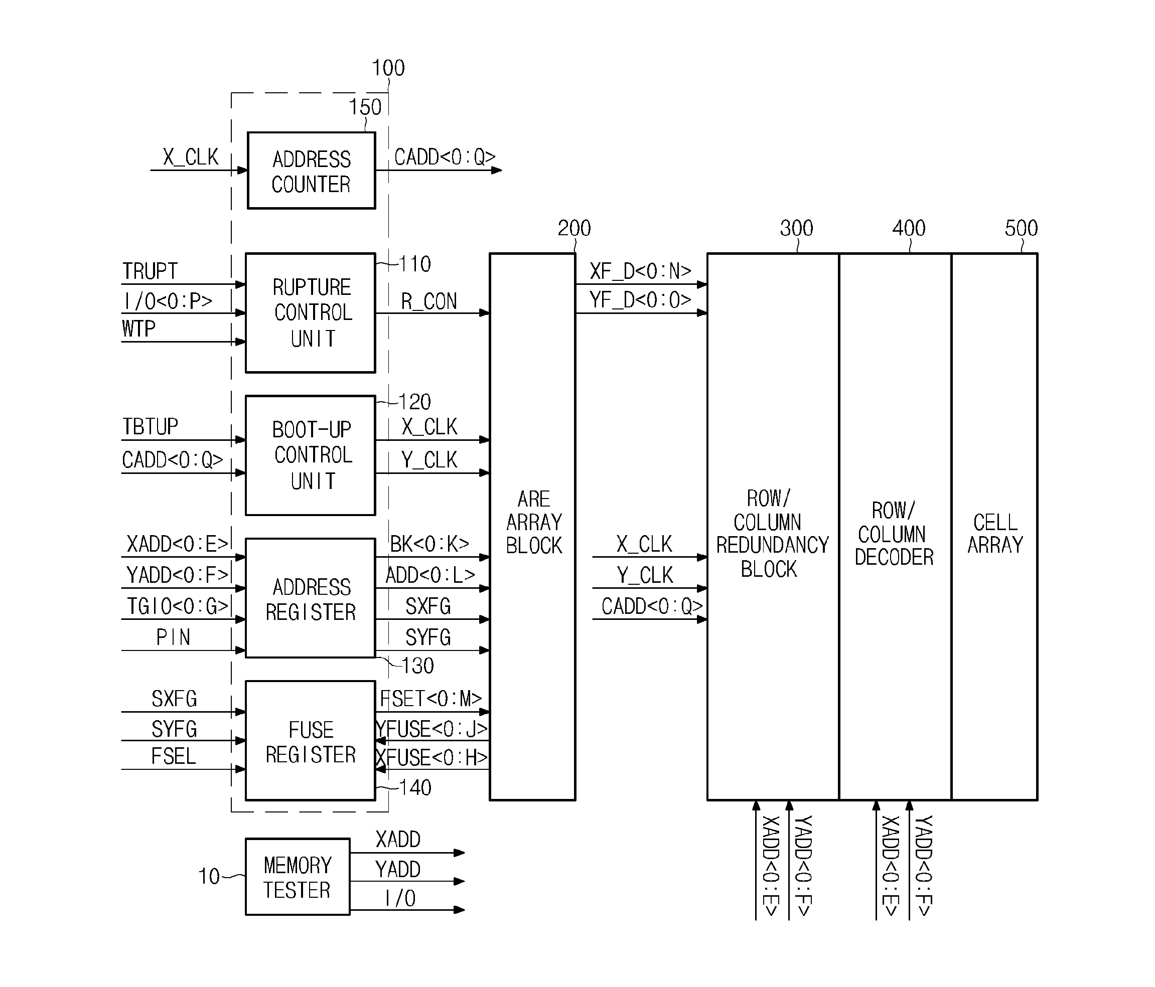
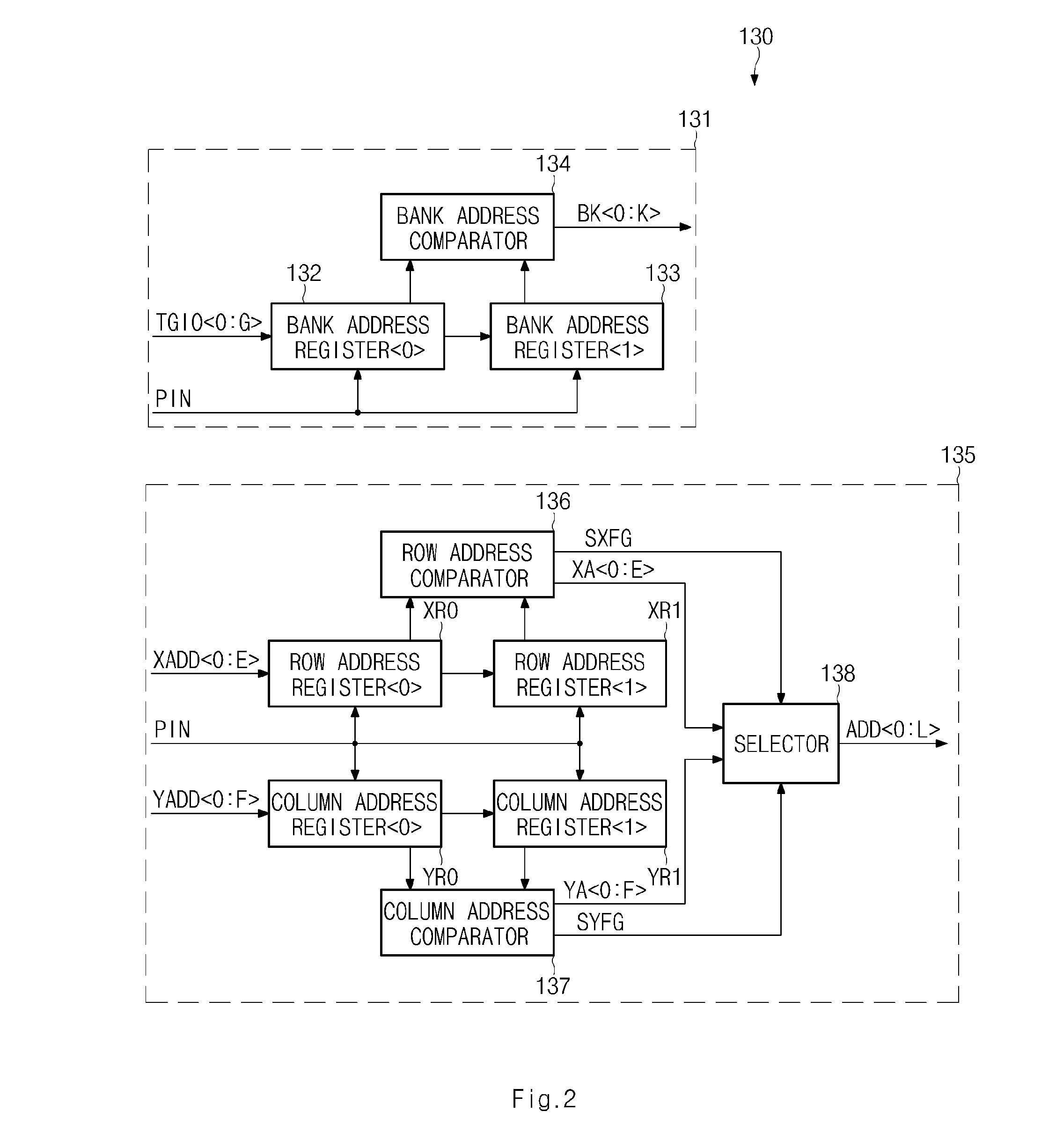
[0029]Hereinafter, a self-repair device according to the invention will be described below with reference to the accompanying drawings through various embodiments.

[0030]As the sizes of respective elements constituting a is semiconductor integrated circuit device gradually decrease and the number of elements included in one semiconductor chip gradually increases, the level of defect density rises. The rise in defect density is a direct factor that lowers the yield of a semiconductor device. If the defect density markedly increases, a wafer on which semiconductor devices are formed should be discarded.

[0031]In order to decrease the defect density, a redundancy circuit which replaces defective cells with redundancy cells has been suggested. In the case of a semiconductor memory device, a redundancy circuit (or a fuse circuit) may be used for each of a row-related line (for example, a word line) and a column-related line (for example, a bit line).

[0032]Such a redundancy circuit includes...


PUM


Abstract

A self-repair device includes an ARE (array rupture electrical fuse) array block configured to store fail addresses; an ARE control block configured to control a repair operation of fuse sets according to the fail addresses, compare a plurality of the fail addresses, and determine a failed state; and a redundancy block configured to store fuse data of the fail addresses, compare an input address with the fail addresses, and control row and column redundancy operations.

Description

CROSS-REFERENCES TO RELATED APPLICATION[0001]The present application claims priority under 35 U.S.C. §119(a) to Korean application number 10-2013-109649, filed on Sep. 12, 2013, in the Korean Intellectual Property Office, which is incorporated herein by reference in its entirety.BACKGROUND[0002]1. Technical Field[0003]Various embodiments relate to a self-repair device, and more particularly, to a technology for improving the repair efficiency and reducing the area of a semiconductor device including a fuse array.[0004]2. Description of Related Art[0005]In general, a semiconductor memory device includes a is number of memory cells. As processing technologies have been developed and thus the degree of integration is augmented, the number of memory cells gradually increases. If a fail occurs in even any one among memory cells, a corresponding semiconductor memory device mis-operates. Therefore, since the semiconductor memory device including a failed cell cannot perform a desired opera...

Claims


Application Information

Patent Timeline
Patent Type & Authority Applications(United States)
IPC IPC(8): G11C29/00G06F11/10
CPCG06F11/1016G11C29/787G11C29/808G11C29/04G11C29/12
Inventor SHIM, YOUNG BO
Owner SK HYNIX INC
Why Eureka
Try Eureka