

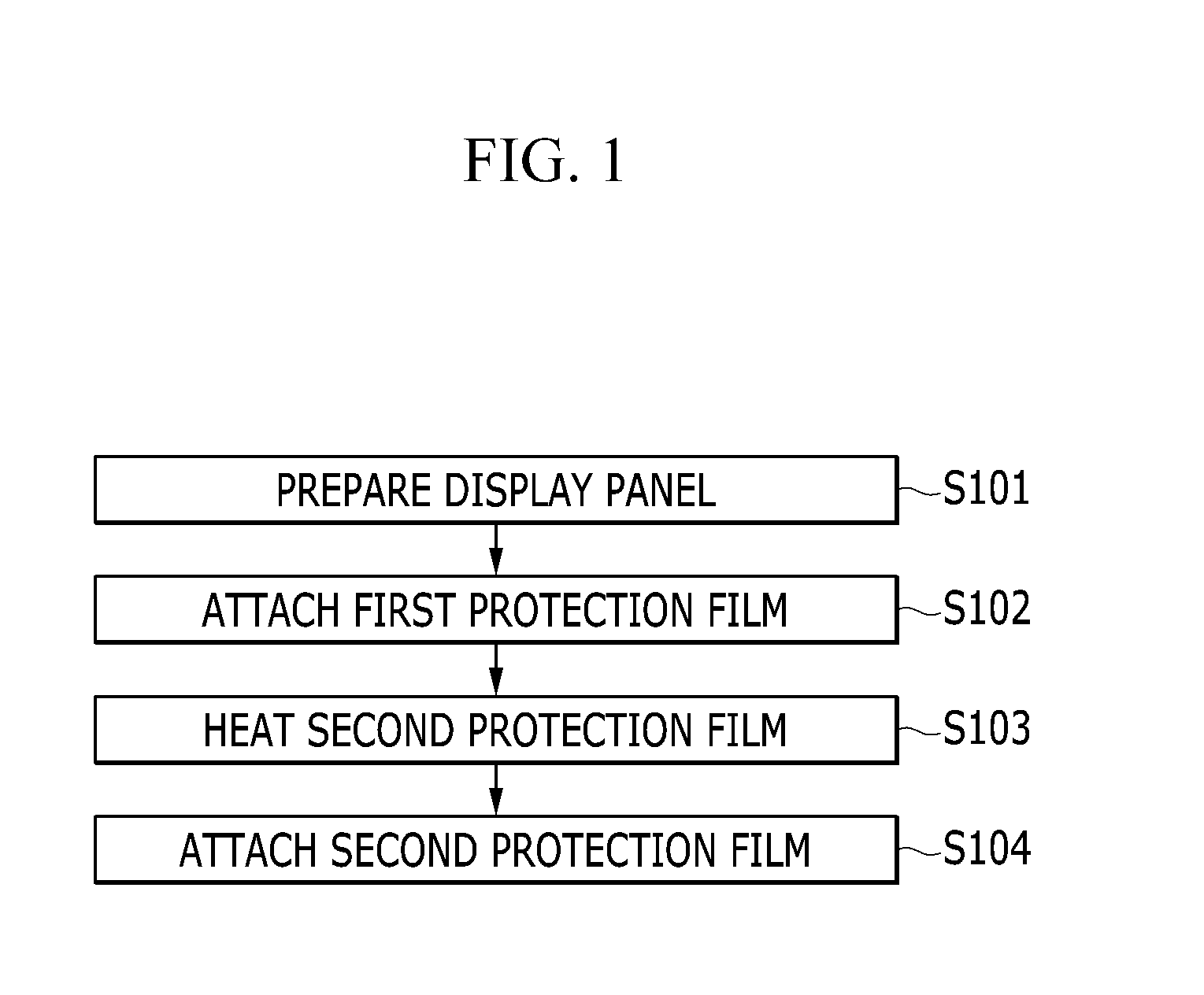
Method of manufacturing an organic light emitting display device
a technology of light-emitting diodes and manufacturing methods, which is applied in the direction of solid-state devices, electric lighting sources, electric light sources, etc., can solve the problems of difficult to perform various subsequent processes and panel bending, and achieve the effect of preventing panel curling
- Summary
- Abstract
- Description
- Claims
- Application Information
AI Technical Summary
Benefits of technology
Problems solved by technology
Method used
Image

Examples
Embodiment Construction
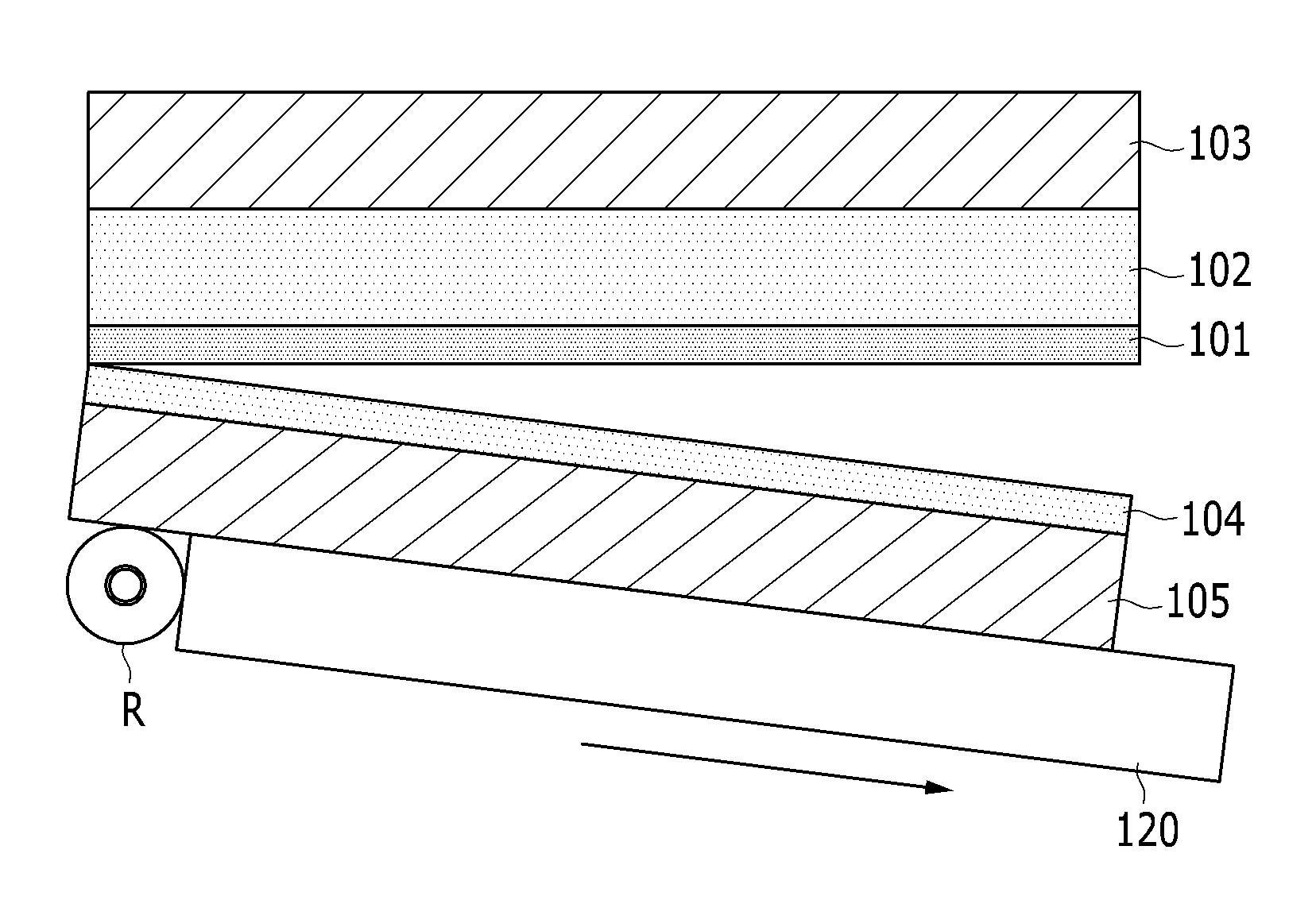
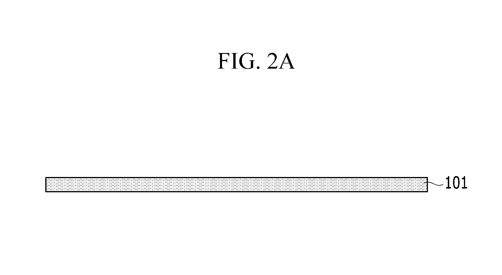
[0024]Hereinafter, exemplary embodiments will be described in detail with reference to the attached drawings such that the present invention can be easily put into practice by those skilled in the art. As those skilled in the art would realize, the described embodiments may be modified in various different ways, all without departing from the spirit or scope of the present invention.
[0025]In addition, in various exemplary embodiments, the same constituent elements are denoted by the same reference numerals and are representatively described in an exemplary embodiment, and different elements from the elements of the exemplary embodiment are described in other exemplary embodiments.
[0026]The drawings are schematic and are not illustrated in accordance with a scale. The relative sizes and ratios of the parts in the drawings are exaggerated or reduced for clarity and convenience in the drawings, and the arbitrary sizes are only exemplary and are not limiting. The same structures, elemen...
PUM
 Abstract
Description
Claims
Application Information