Photovoltaic device and method of manufacturing the same

Inactive Publication Date: 2015-04-09
SINO AMERICAN SILICON PROD
View PDF4 Cites 20 Cited by
  • Summary
  • Abstract
  • Description
  • Claims
  • Application Information

AI Technical Summary

Benefits of technology

[0009]The object of the instant disclosure is to provide a photovoltaic device

Problems solved by technology

Emphasis on reliability problems of photovoltaic devices and package module thereof resulted from PID effect are becoming more evident.
That package module is conditioned under long-term high temperature, humid surroundings, and high voltage that lead to current leakage between the glass material and the package module.

Method used


Image

  • Photovoltaic device and method of manufacturing the same
  • Photovoltaic device and method of manufacturing the same
  • Photovoltaic device and method of manufacturing the same

Examples


Embodiment Construction

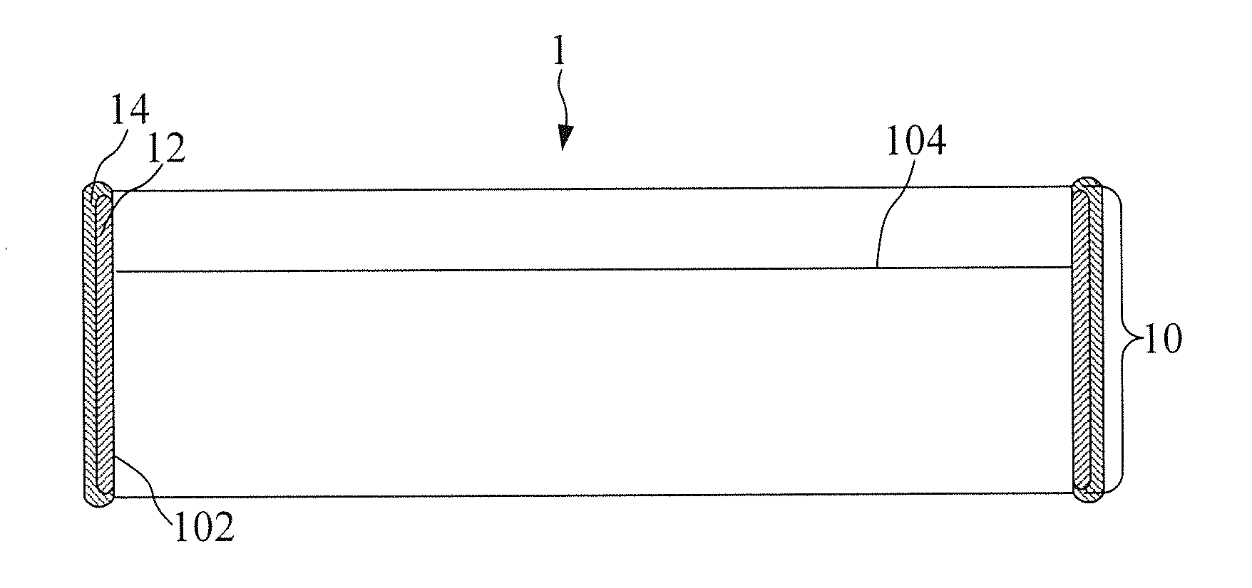
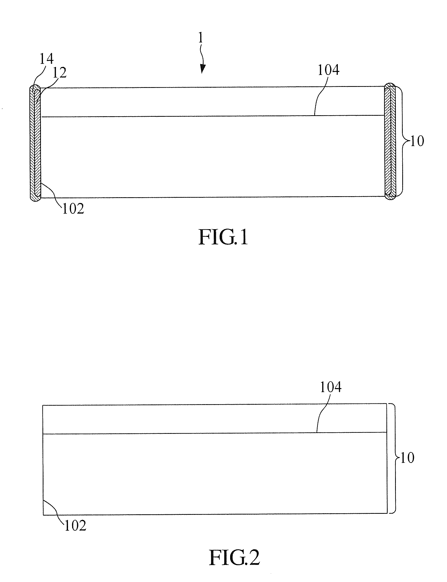
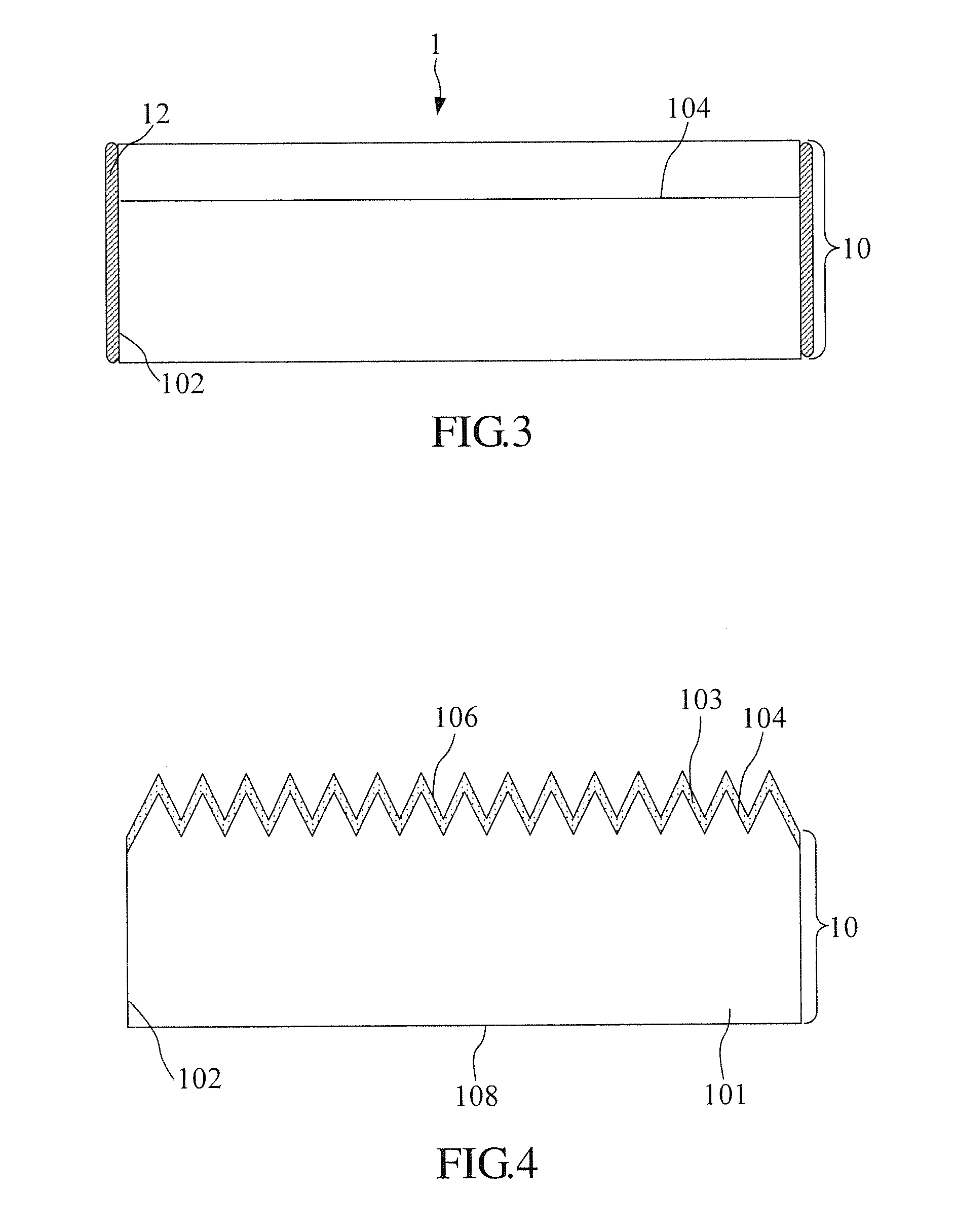
[0021]Please refer to FIG. 1 as a cross-sectional view of the photovoltaic device 1 from one preferred embodiment in the instant disclosure.

[0022]As FIG. 1 shows, the instant disclosure provides the photovoltaic device 1 including a semiconductor structure assembly 10 and a first protection layer 12. The semiconductor structure assembly 10 has a plurality of side surfaces 102 that include p-n junction, n-p junction, p-i-n junction, n-i-p junction, double junction, and multiple junction, or junctions of other types. In other words, the photovoltaic device 1 can be a monolithic silicon photovoltaic device, a monolithic silicon liked photovoltaic device, a poly-silicon photovoltaic device, a gallium arsenide photovoltaic device, an amorphous silicon thin film photovoltaic device, a □-silicon thin film photovoltaic device, a Cadmium sulfide (CdS) photovoltaic device, a Cadmium telluride (CdTe) thin film photovoltaic device, CuInSe2 (CIS) thin film photovoltaic device, Cu(In, Ga)Se2 (CIG...


PUM


Abstract

The invention provides a photovoltaic device and method of manufacturing the same. The photovoltaic device of the invention includes a semiconductor structure assembly and a protection layer. The semiconductor structure assembly has a plurality of side surfaces, and includes a p-n junction, an n-p junction, a p-i-n junction, an n-i-p junction, a tandem junction or a multi-junction. In particular, the protection layer is formed to overlay the sides of the semiconductor structure assembly. Thereby, the protection layer can effectively inhibit the potential-induced degradation effect of the photovoltaic device of the invention.

Description

CROSS REFERENCE TO RELATED APPLICATIONS[0001]This Application is a Continuation-in-Part of application Ser. No. 13 / 924,752, filed Jun. 24, 2013, now pending, and entitled SOLAR CELL AND METHOD OF MANUFACTURING THE SAME.BACKGROUND OF THE INSTANT DISCLOSURE[0002]1. Field of the Invention[0003]The instant disclosure relates to a photovoltaic device and method of manufacturing the same; in particular, to the photovoltaic device effectively inhibiting potential-induced degradation (PID) effect and method of manufacturing the same.[0004]2. Description of Related Art[0005]Emphasis on reliability problems of photovoltaic devices and package module thereof resulted from PID effect are becoming more evident. Manufacturers devote themselves into development of photovoltaic devices and package module thereof capable of inhibiting PID. PID effect was first discovered from n-type silicon substrate based photovoltaic devices by the Sunpower company in 2005. That package module is conditioned under...

Claims


Application Information

Patent Timeline
IPC IPC(8): H01L31/0203H01L31/0236H01L31/02H01L31/0216
CPCH01L31/0203H01L31/0201H01L31/02366H01L31/02168H01L31/022425H01L31/1804H01L31/02167H01L31/02363Y02E10/547Y02P70/50
Inventor TJAHJONO, BUDIYANG, MING-JUITING, CHUAN-WENWU, WEN SHENGSHEN, KUO-WEILIU, CHIEN HONG
Owner SINO AMERICAN SILICON PROD
Why Eureka
Try Eureka