Substrate plate for MEMS devices

a technology of mems devices and substrate plates, applied in the field of substrate plates, can solve the problems of interfering with the electrical connection between the extra contact pads and the associated contact pads in the footprint, and achieve the effect of high efficiency

Active Publication Date: 2015-04-16
OCE TECH
View PDF4 Cites 20 Cited by
  • Summary
  • Abstract
  • Description
  • Claims
  • Application Information

AI Technical Summary

Benefits of technology

[0015]Using the extra contact pad instead of the regular contact pads within the footprint of the MEMS device has the advantage that the regular contact pads need not be used in the manufacturing and / or test process, which avoids a risk of these contact pads being damaged before the permanent bonds are established in the packaging process.
[0016]According to an embodiment, the present invention further offers the advantageous possibility to use the extra contact pad for short-circuiting a plurality of components of the MEMS device, or even of a plurality of MEMS devices formed on the same wafer, in order to apply a common process or test signal to these components and / or to measure an output voltage or current of these components with high efficiency, because only a single electrical contact has to be established for this purpose. When a plurality of MEMS devices formed on the same wafer is short-circuited, a lead structure may connect the extra contact pad with a plurality of contact pads of a plurality of components of different MEMS devices. At least a major part of the extra contact pad may be located within the footprint of one of said MEMS devices.

Problems solved by technology

Since the lead structure extends outside of the footprint of the MEMS device, it will be cut away when the substrate plate is diced, thereby interrupting the electrical connection between the extra contact pad and the associated contact pad in the footprint of the MEMS device.

Method used


Image

  • Substrate plate for MEMS devices
  • Substrate plate for MEMS devices
  • Substrate plate for MEMS devices

Examples


Embodiment Construction

[0028]The present invention will now be described with reference to the accompanying drawings, wherein the same or similar elements are identified with the same reference numeral.

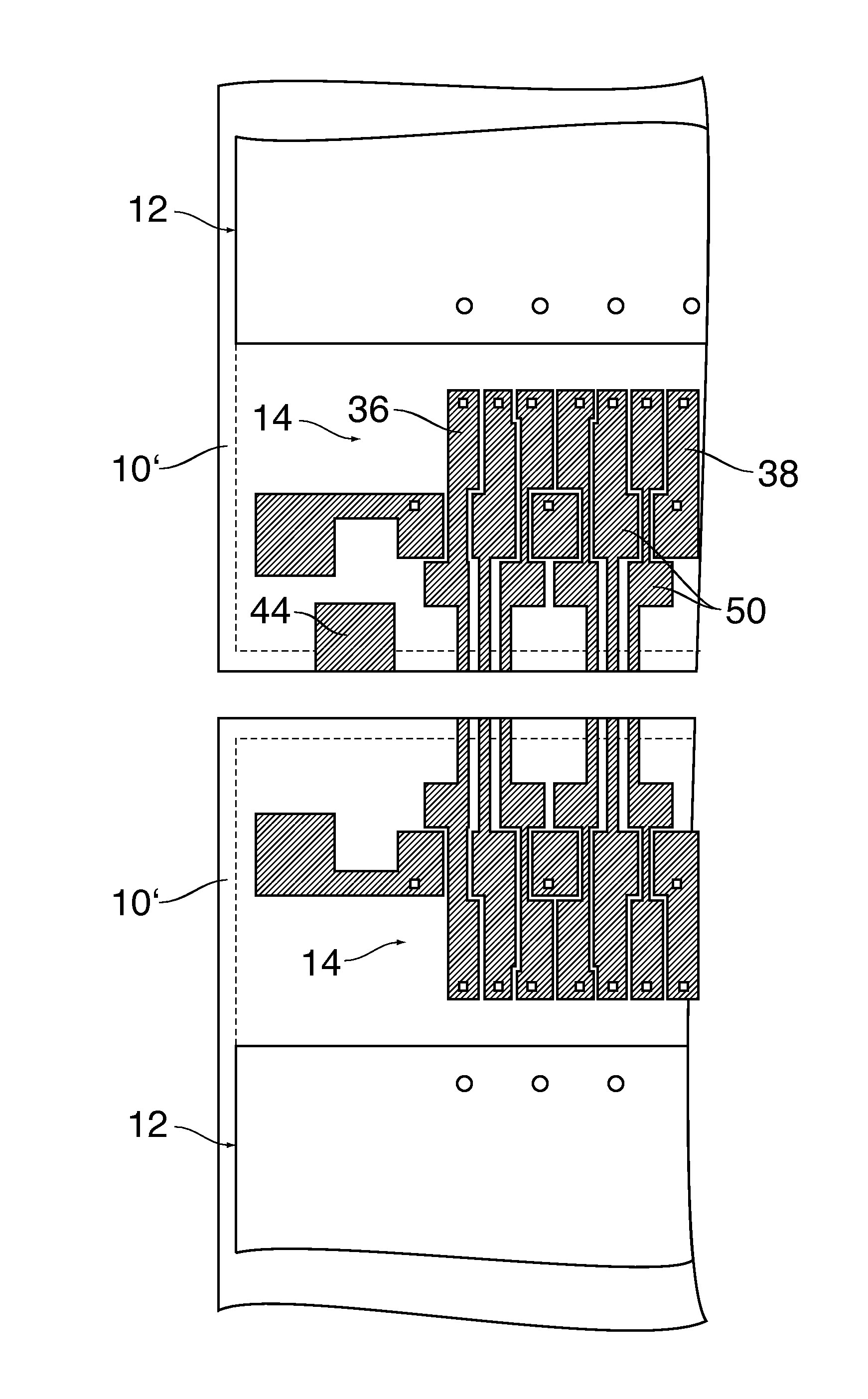
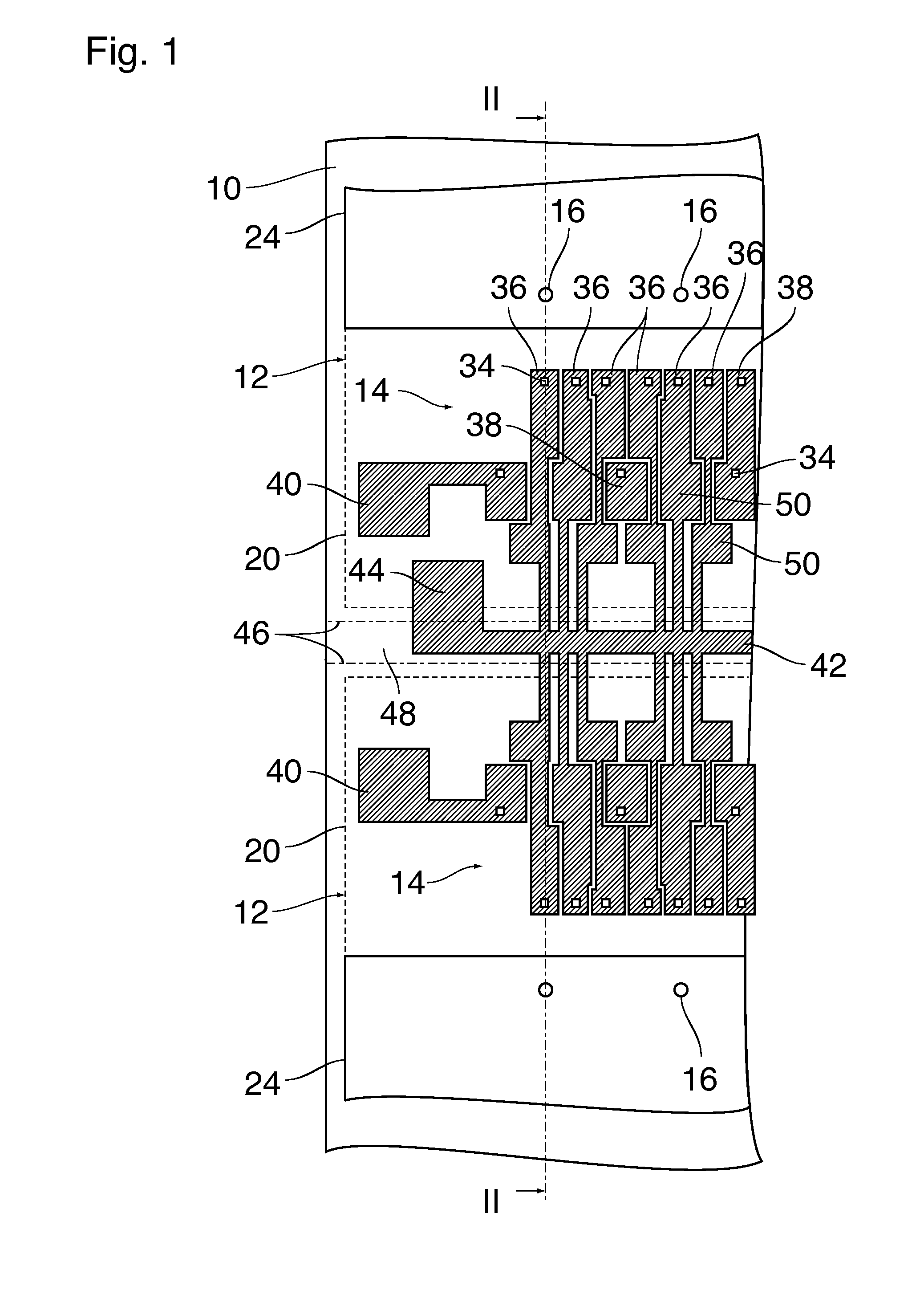
[0029]In FIG. 1, a portion of a substrate plate 10 has been shown on which two MEMS devices 12 have been formed. A pattern 14 of electrically conductive leads is formed on one surface of the substrate plate 10 for contacting the electric components of the MEMS devices 12. The MEMS devices 12 and the patterns 14 are arranged mirror-symmetrically in this example.

[0030]By way of example, each of the MEMS devices 12 constitutes a piezoelectric ink jet print head, which comprises a plurality of nozzles 16.

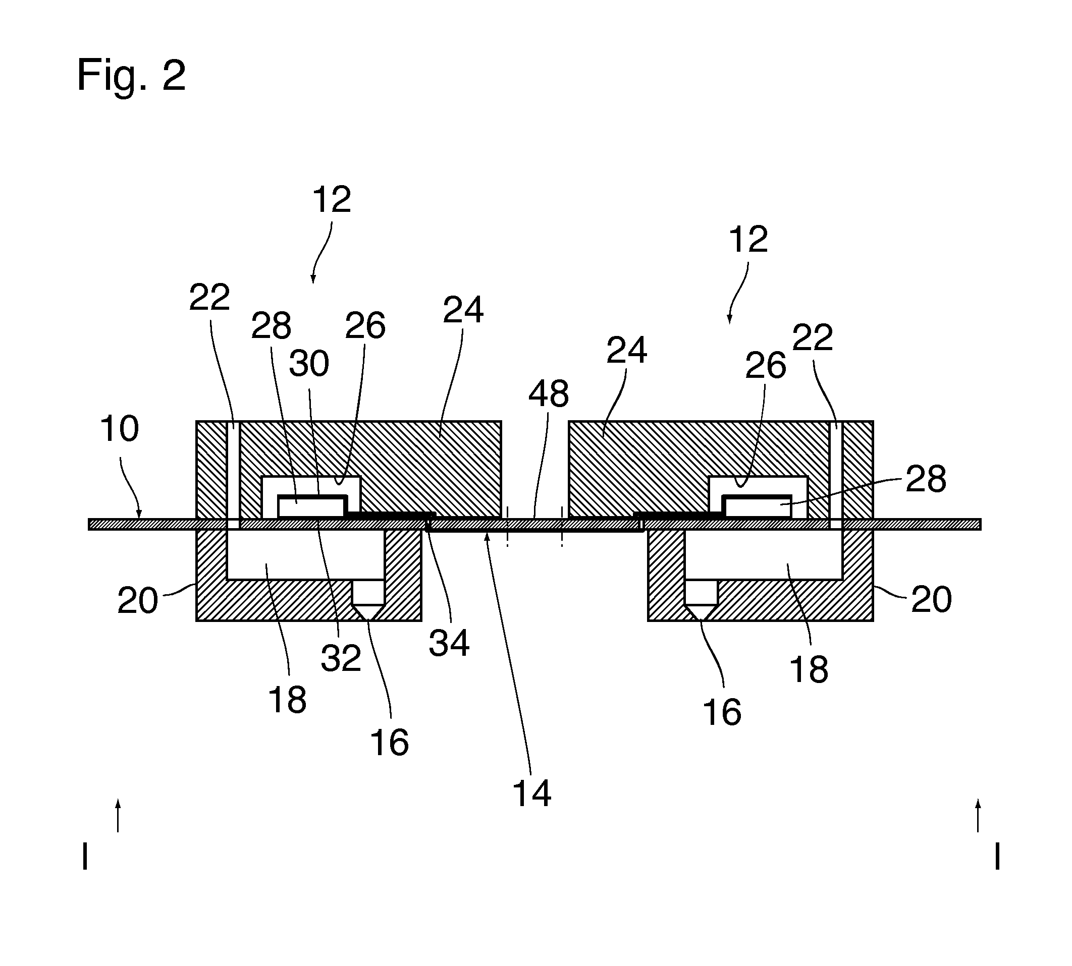
[0031]As can be seen more clearly in FIG. 2, each of the nozzles 16 is connected to an ink chamber 18 that is formed in a chamber block 20 of the MEMS device 12 and is connected to an ink duct 22 via an opening formed in the substrate plate 10. The ink duct 22 is formed in a duct block 24 that also forms an act...


PUM

PropertyMeasurementUnit
widthaaaaaaaaaa
widthaaaaaaaaaa
electrically conductiveaaaaaaaaaa

Abstract

A substrate plate is provided for at least one MEMS device to be mounted thereon. The MEMS device has a certain footprint on the substrate plate, and the substrate plate has a pattern of electrically conductive leads to be connected to electric components of the MEMS device. The pattern forms contact pads within the footprint of the MEMS device and includes at least one lead structure that extends on the substrate plate outside of the footprint of the MEMS device and connects a number of the contact pads to an extra contact pad. The lead structure is a shunt bar that interconnects a plurality of contact pads of the MEMS device and is arranged to be removed by means of a dicing cut separating the substrate plate into a plurality of chip-sized units. At least a major part of the extra contact pad is formed within the footprint of one of the MEMS devices.

Description

CROSS-REFERENCE TO RELATED APPLICATIONS[0001]This application claims priority under 35 U.S.C. §119(a) to Application No. 13188352.2, filed in Europe on Oct. 11, 2013, the entirety of which is expressly incorporated herein by reference.BACKGROUND OF THE INVENTION[0002]1. Field of the Invention[0003]The present invention relates to a substrate plate for at least one MEMS device to be mounted thereon. The MEMS device has a certain footprint on the substrate plate, and the substrate plate has a pattern of electrically conductive leads to be connected to electric components of the MEMS device. The pattern forms contact pads within the footprint of the MEMS device and comprises at least one lead structure that extends on the substrate plate outside of the footprint of the MEMS device and connects a number of said contact pads to an extra contact pad. The lead structure is a shunt bar that interconnects a plurality of contact pads of the MEMS device and is arranged to be removed by means o...

Claims


Application Information

Patent Timeline
Patent Type & Authority Applications(United States)
IPC IPC(8): B81C99/00G01R31/02G01R31/26B81C1/00H05K1/11G01R31/50
CPCB81C99/004B81C1/00301H05K1/111G01R31/2601G01R31/02H05K2201/09372B81B2207/03B81B7/007B81B2201/052B41J2/14233B41J2/161B41J2/1632B41J2002/14241B41J2002/14491H05K1/0268B41J2/1635B41J2002/14459G01R31/50
Inventor HUYGENS, MAIKEL A.J.VAN DER MEER, RENE J.PANNEKOEK, REINIERWESTLAND, ALEX N.
Owner OCE TECH
Why Eureka
Try Eureka