

Wiring board and method of manufacturing the same
a wiring board and wire technology, applied in the field of wiring boards, can solve the problems that the conductor pillar b>112/b> cannot be formed successfully, and achieve the effect of increasing the filling pressure and reducing the viscosity
- Summary
- Abstract
- Description
- Claims
- Application Information
AI Technical Summary
Benefits of technology
Problems solved by technology
Method used
Image

Examples
Embodiment Construction
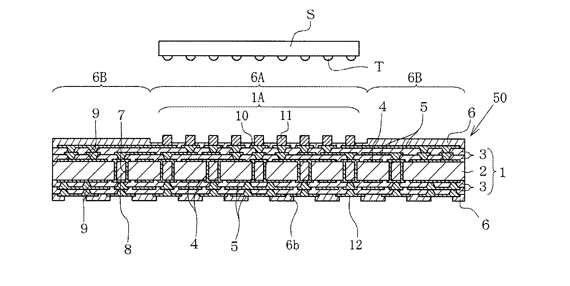
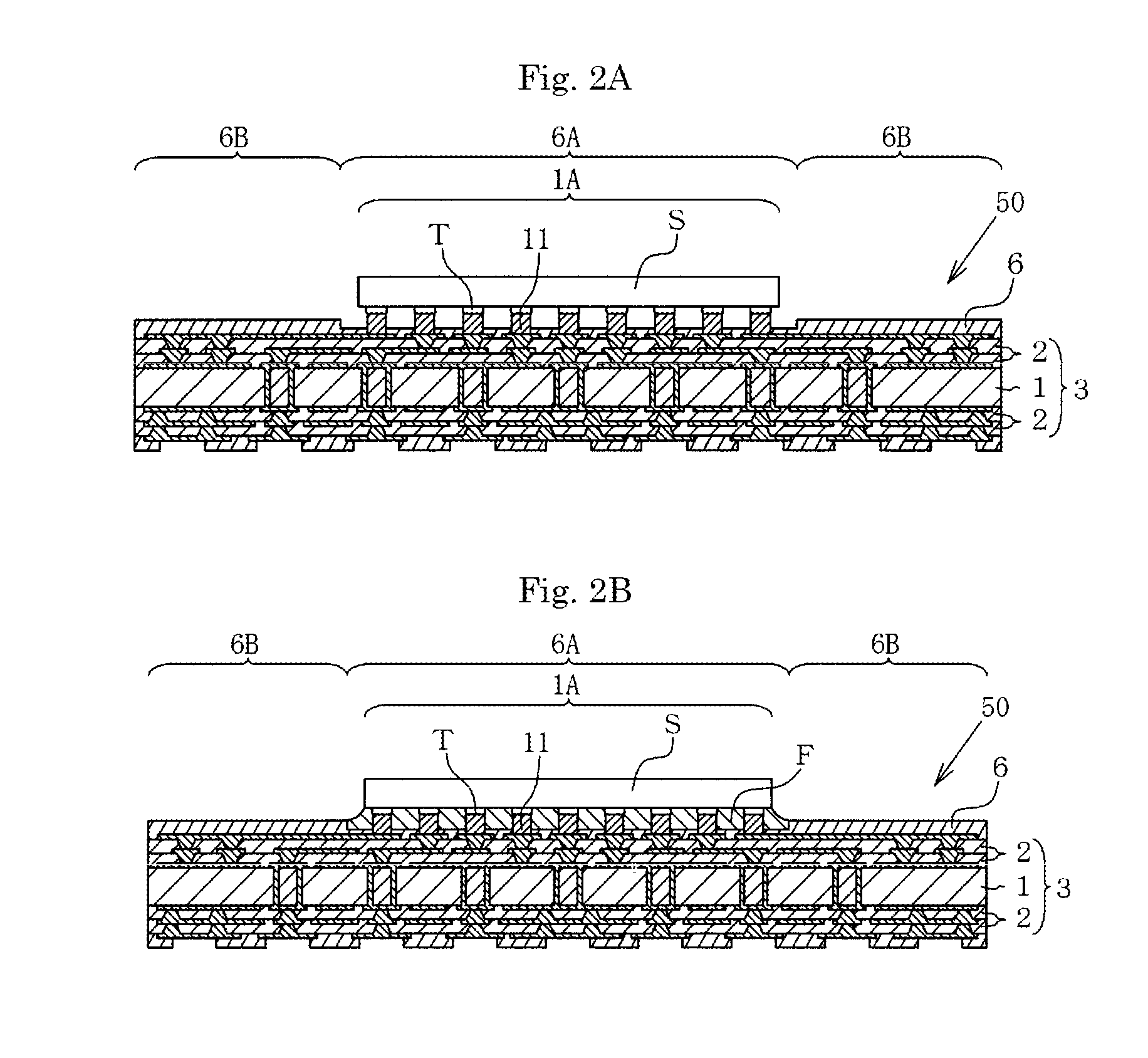
[0030]The following is a description of a wiring board and a manufacturing method therefor according to the present invention, with reference to drawings attached hereto. A wiring board 50 shown in FIG. 1 is a wiring board according to an embodiment of the present invention. An area-array-type semiconductor element S is mounted on the wiring board 50 by flip chip connection.
[0031]As shown in FIG. 1, the wiring board 50 has a mounting portion 1A on an upper surface of an insulating board 1. The semiconductor element S is mounted on the mounting portion 1A. On the mounting portion 1A, there are formed a number of semiconductor element connection pads 10. In a central part of an upper surface of each of the semiconductor element connection pads 10, there is formed a columnar conductor pillar 11. The conductor pillars 11 are arranged in an array corresponding to an array of electrode terminals T of the semiconductor element S. A lower surface of the insulating board 1 is an external con...
PUM
| Property | Measurement | Unit |
|---|---|---|
| height | aaaaa | aaaaa |
| height | aaaaa | aaaaa |
| height | aaaaa | aaaaa |
Abstract
Description
Claims
Application Information