Inkjet apparatus and method for manufacturing organic el device

Active Publication Date: 2015-04-30
PANASONIC INTELLECTUAL PROPERTY MANAGEMENT CO LTD
View PDF5 Cites 4 Cited by
  • Summary
  • Abstract
  • Description
  • Claims
  • Application Information

AI Technical Summary

Benefits of technology

The invention relates to an inkjet device that reduces the length of collateral vapor bubbles (ligaments) and the occurrence of satellite mist in ink drops. This is achieved by applying a standby oscillation to the ink interface in the nozzle to create a stable vibration pattern that interferes with the main oscillation required for ink drops to escape. The device allows for high flexibility in setting the pressure required to induce ink discharge while maintaining a low ligament length.

Problems solved by technology

However, there is a problem of unsuitable landing associated with satellite mist, which is as an impediment to landing accuracy.
Specifically, for an organic electroluminescence device such as a display panel, the occurrence of satellite mist in the manufacturing process causes many minute ink drops to land at positions other than intended, which eventually leads to display failure.
However, ink viscosity also influences ligament shape, such that the lower the ink viscosity, the more likely the ligament is to disperse while still elongating.
In terms of discharge speed specifics, given that the discharge speed is lowered when the magnitude of the drive voltage signal is reduced, the discharged drive ink drops are prone to swaying due to stream effects and the like, which leads to new problems of inaccurate landing.
Therefore, the actual range of usable drive voltage signal is limited.

Method used


Image

  • Inkjet apparatus and method for manufacturing organic el device
  • Inkjet apparatus and method for manufacturing organic el device
  • Inkjet apparatus and method for manufacturing organic el device

Examples


embodiment 1

[0101]The following describes an inkjet device pertaining to the present Embodiment, with reference to the accompanying drawings.

[0102]

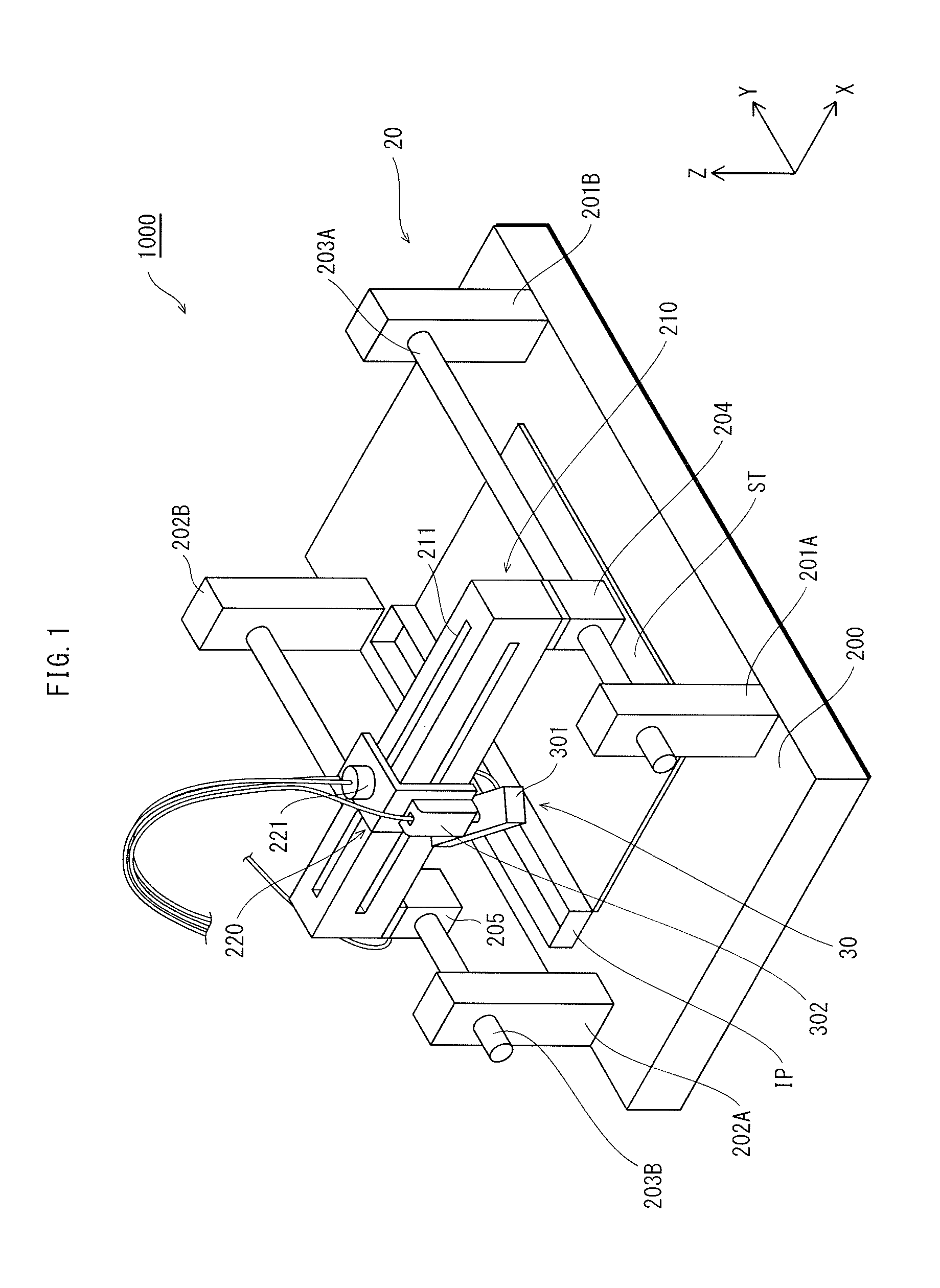
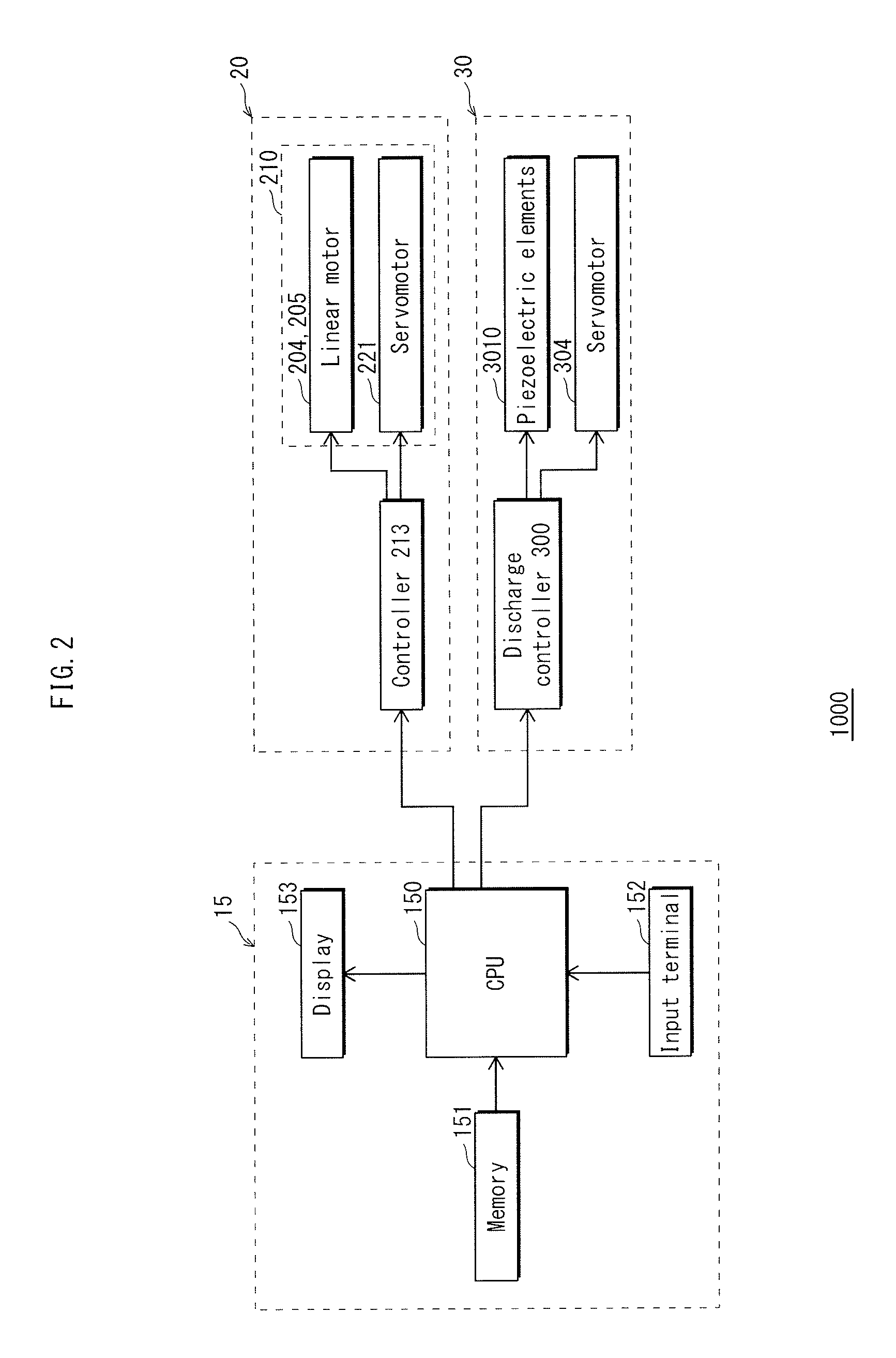
[0103]FIG. 1 illustrates the main configuration of an inkjet device 1000 pertaining to the Embodiment. FIG. 2 is a functional block diagram of the inkjet device 1000.

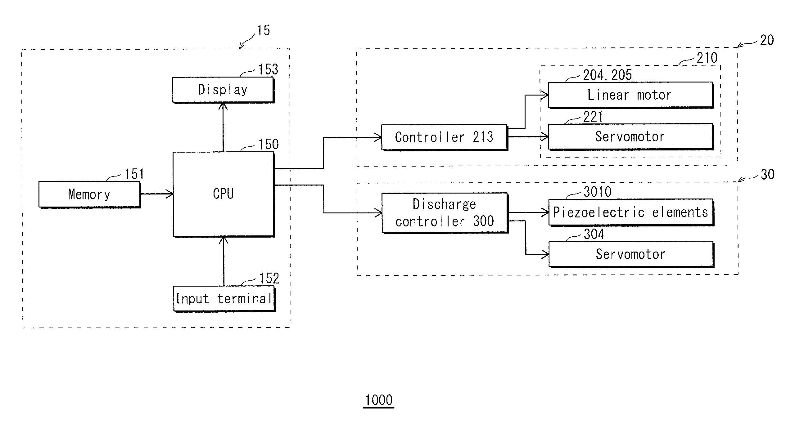
[0104]As shown in FIGS. 1 and 2, the inkjet device 1000 includes an inkjet table 20, a head 30, and a control device 15.

[0105]The inkjet device 1000 is illustrated as having an inkjet head 301 on a single head 30. However, no such limitation is intended. For example, the inkjet head 301 may be provided in plurality by having a plurality of inkjet heads 301 provided a single head 30, or one or more inkjet heads 301 may be provided on each of a plurality of heads 30, or any of various other forms.

[0106]As shown in FIG. 2, the control device 15 includes a central processing unit (hereinafter, CPU) 150, a memory 151 (such as a hard disk drive or similar large-capacity memory), a display 153,...

embodiment 2

[0190]First, the configuration of an organic electroluminescence device manufactured using the method pertaining to the present Embodiment is described, prior to explaining the manufacturing method for the organic electroluminescence device pertaining to the present Embodiment.

[0191]

[0192]FIG. 11 is a partial cross-sectional diagram indicating the configuration of the organic electroluminescence device to which the manufacturing method of the present Embodiment applies. The organic electroluminescence device 100 of FIG. 11 is illustrated as an organic electroluminescence panel on which are disposed a plurality of organic electroluminescence elements 115. However, a single organic electroluminescence element may be provided alone on the organic electroluminescence device. The organic electroluminescence device 100 of FIG. 11 is intended only as an example.

[0193]In FIG. 11, the organic electroluminescence device 100 is oriented such that the top of the page is the display surface. Tha...


PUM


Abstract

An inkjet device includes an inkjet head having a pressure applier applying voltage to ink contained in a ink reservoir, by executing a standby drive operation of applying a standby oscillation to the ink and a main drive operation of applying a main oscillation to cause the ink to be discharged from nozzles, such that the start of main drive operation execution is within a period where the displacement in the standby oscillation is oriented toward the interior of the nozzles in order to produce interference between the standby oscillation.

Description

TECHNICAL FIELD[0001]The present disclosure pertains to an inkjet device and to an organic electroluminescence device using the inkjet device.BACKGROUND ART[0002]Many drive schemes for causing ink discharge have been proposed for inkjet devices, including a pump scheme, a piezoelectric scheme, a thermal scheme, and so on. For example, in the piezoelectric scheme, a drive signal (i.e., a drive voltage signal) is applied to voltage elements in order to cause ink discharge by causing an ink reservoir to expand and contract, which applies pressure to the ink within the ink reservoir and causes ink drops to be discharged from nozzles.[0003]In recent years, application technology used in inkjet device is expected to be adapted to device manufacturing, such as for organic electroluminescence devices. Improvements to the landing accuracy of ink drops are thus demanded for increasing device precision.[0004]An impediment to landing accuracy improvements is the problem of satellite mist. This ...

Claims


Application Information

Patent Timeline
IPC IPC(8): B41J2/045H01L51/00H01L51/56
CPCB41J2/04588H01L51/0005H01L51/56B41J2/04581B41J2/04516B41J2202/09H10K59/122H10K71/135H10K71/00
Inventor TAKATA, MASAKAZUNANNO, HIROTAKA
Owner PANASONIC INTELLECTUAL PROPERTY MANAGEMENT CO LTD
Why Eureka
Try Eureka