Method for forming metal circuit, liquid trigger material for forming metal circuit and metal circuit structure

a metal circuit and liquid trigger technology, applied in metal pattern materials, railway components, nuclear engineering, etc., can solve problems such as unsuitability for high-frequency antennas

Active Publication Date: 2015-05-07
IND TECH RES INST
View PDF13 Cites 6 Cited by
  • Summary
  • Abstract
  • Description
  • Claims
  • Application Information

AI Technical Summary

Benefits of technology

[0008]According to one embodiment, a liquid trigger material that is curable and suitable for forming a metal circuit is provided. The liquid trigger material comprises: an insulating gel comprised of a macromolecular material that is curable; and a plurality of trigger particles comprised of at least one of organometallic particles, a chelation, and a semiconductor material having an energy gap greater than or equal to 3 eV, the trigger particles being activated when irradiated by a laser having a first wavelength; wherein, the trigger particles are distributed in the insulating gel, such that the liquid trigger material has a viscosity of less than 10000 cP The liquid trigger material, after curing, has a dielectric constant between 2 and 6.5.

Problems solved by technology

However, the LDS technology is applicable to only certain plastic substrates, with a limited range of dielectric constants, and thereby is not suitable for high-frequency antennas.

Method used


Image

  • Method for forming metal circuit, liquid trigger material for forming metal circuit and metal circuit structure
  • Method for forming metal circuit, liquid trigger material for forming metal circuit and metal circuit structure
  • Method for forming metal circuit, liquid trigger material for forming metal circuit and metal circuit structure

Examples


Embodiment Construction

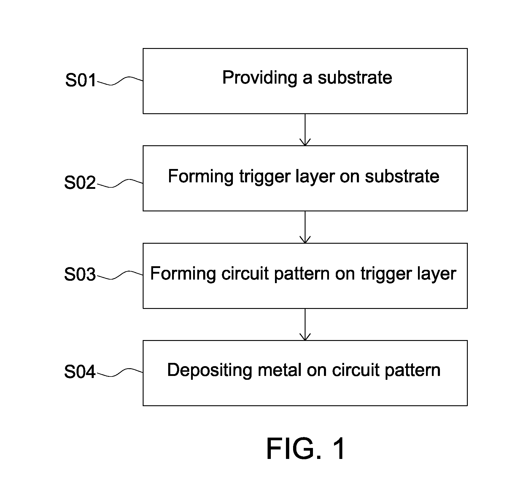
[0017]FIG. 1 shows a flowchart of a method for forming a metal circuit according to an embodiment. As shown in FIG. 1, the method includes steps S01 to S04. In step S01, a substrate is provided. In step S02, a trigger layer is formed on the substrate. In step S03, a circuit pattern is formed on the trigger layer. In step S04, a metal is deposited on the circuit pattern. With the above method, a single-layer or multi-layer metal circuit can be formed on the substrate.

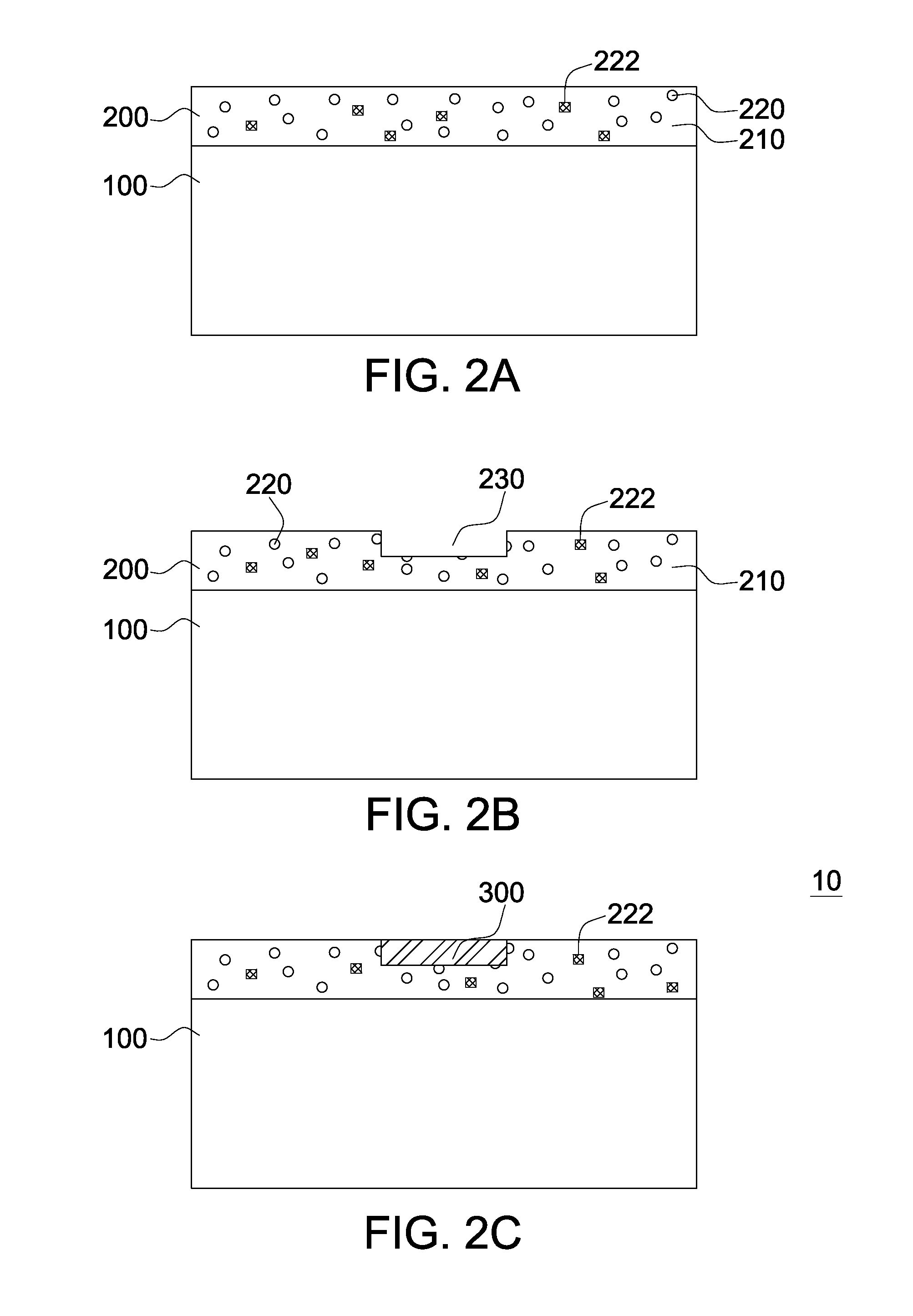
[0018]Details of the steps of the method for forming a metal circuit in FIG. 1 are given with reference to FIGS. 2A to 2C below.

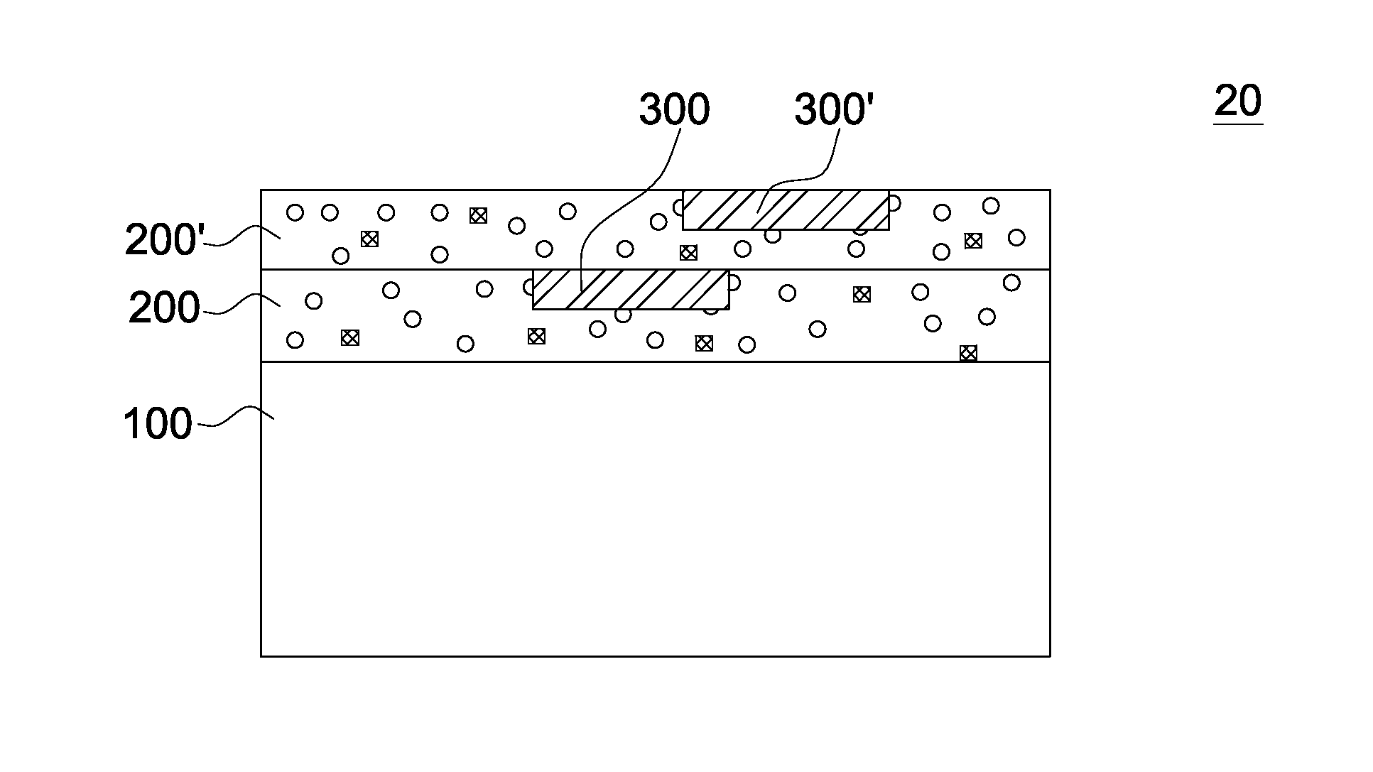
[0019]As shown in FIG. 2A, a substrate 100 is provided, and a first trigger layer 200 is formed on the substrate 100. The substrate 100 may be made of a conductive material or a non-conductive material. In the embodiment, the substrate 100 has a flat surface. In practice, the first trigger layer 200 may be formed on a substrate 100 having any shape to form a stereoscopic metal circuit structure....


PUM

PropertyMeasurementUnit
energy gapaaaaaaaaaa
viscosityaaaaaaaaaa
dielectric constantaaaaaaaaaa

Abstract

A metal circuit structure, a method for forming a metal circuit and a liquid trigger material for forming a metal circuit are provided. The metal circuit structure includes a substrate, a first trigger layer and a first metal circuit layer. The first trigger layer is disposed on the substrate and includes a first metal circuit pattern. The first metal circuit layer is disposed on the first circuit pattern and is electrically insulated from the substrate. The composition of the first trigger layer includes an insulating gel and a plurality of trigger particles. The trigger particles are at least one of organometallic particles, a chelation and a semiconductor material having an energy gap greater than or equal to 3 eV. The trigger particles are disposed in the insulating gel, such that the dielectric constant of the first trigger layer after curing is between 2 and 6.5.

Description

CROSS-REFERENCE TO RELATED APPLICATION[0001]This application claims the benefit of Taiwan Application Serial No. 102139840, filed Nov. 1, 2013, the disclosure of which is incorporated by reference herein in its entirety.BACKGROUND OF THE INVENTION[0002]1. Field of the Invention[0003]The disclosure relates in general to a metal circuit structure, a method for forming a metal circuit and a liquid trigger material for forming a metal circuit, and more particularly, to a method for forming a metal circuit on a substrate by electroless plating, a liquid trigger material applied for electroless plating and a metal circuit structure formed using the same.[0004]2. Background of the Related Art[0005]To integrate more functions into a single portable electronic device or to miniaturize the size of a portable electronic device, developers and manufacturers strive to reduce the volume of components inside the device. For example, transceiving antennas previously dominated by printed circuit boa...

Claims


Application Information

Patent Timeline
Patent Type & Authority Applications(United States)
IPC IPC(8): H05K1/09C23C18/16H05K3/18C09D5/24
CPCH05K1/092C09D5/24H05K2201/032H05K3/182C23C18/1651C23C18/165H05K3/4661H05K3/107H05K3/185H05K3/4676C23C18/1608C23C18/1612H05K1/0296H05K1/0373H05K2201/0209
Inventor KAO, TUNE-HUNEHUANG, MENG-CHICHOU, MIN-CHIEH
Owner IND TECH RES INST
Why Eureka
Try Eureka