Particle generation suppresspr by DC bias modulation

a technology of dc bias modulation and particle generation, which is applied in the direction of plasma technique, electric discharge lamp, coating, etc., can solve the problems of unwanted particle contamination on the substrate surface, ion bombardment of the powered electrode, and the portion of the protective coating layer may fall off, so as to reduce particle generation and reduce particle generation in the processing chamber

Active Publication Date: 2015-05-07
APPLIED MATERIALS INC
View PDF13 Cites 85 Cited by
  • Summary
  • Abstract
  • Description
  • Claims
  • Application Information

AI Technical Summary

Problems solved by technology

It has been observed that one of conventional plasma processing chamber designs in which the plasma is generated between two parallel electrodes positioned over a gas distribution plate can cause unwanted particle contamination on a substrate surface due to ion bombardment of the electrodes.
This sheath voltage causes positive ions within the plasma to accelerate toward the powered electrode, resulting in ion bombardment of the powered electrode.
In instances where the powered electrode includes a protective coating layer, a portion of the protective coating layer may flake off as a result of the ion bombardment and contaminate the substrate surface.
While a lower input power can be used to generate the plasma (and thus reduce particle contamination), the film deposition rate will be decreased, which in turn lowers the process yield.

Method used


Image

  • Particle generation suppresspr by DC bias modulation
  • Particle generation suppresspr by DC bias modulation
  • Particle generation suppresspr by DC bias modulation

Examples


Embodiment Construction

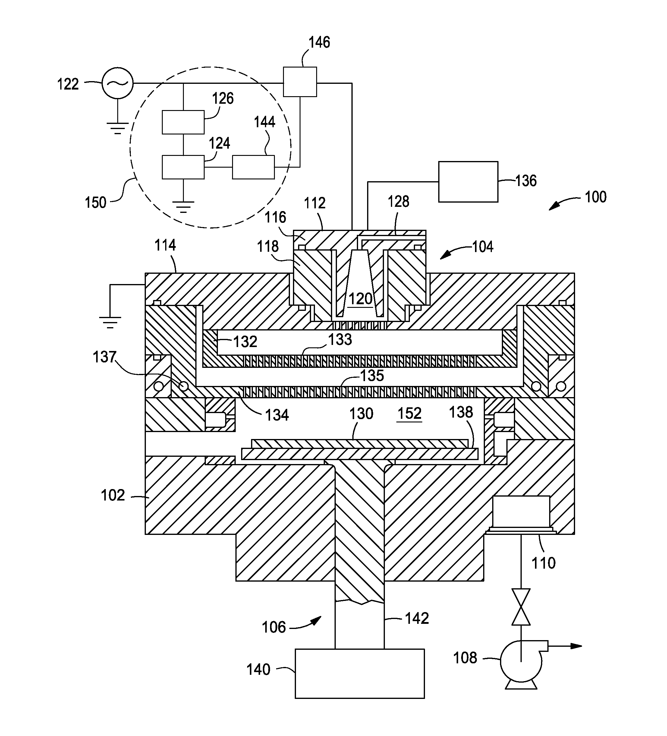
[0018]Embodiments of the present disclosure generally relate to an apparatus and method for reducing particle generation in a processing chamber. The method generally includes generating a plasma between a top electrode and a bottom electrode, and applying a zero DC bias voltage to the top electrode so that the top electrode is operated with a constant zero DC bias voltage during a film deposition process. In another embodiment, an apparatus for processing a substrate is provided. The apparatus generally includes a lid assembly disposed above a chamber body. The lid assembly has a top powered electrode and a grounded bottom electrode disposed parallel to the top powered electrode, defining a plasma volume therebetween. A low-pass filter is disposed between the lid assembly and a RF power supply and configured to direct DC bias to ground so that the top electrode (RF hot) is operated at a constant zero DC bias voltage during a film deposition process.

[0019]Applying zero DC bias volta...


PUM

PropertyMeasurementUnit
poweraaaaaaaaaa
frequencyaaaaaaaaaa
frequencyaaaaaaaaaa

Abstract

Embodiments of the present disclosure generally relate to an apparatus and method for reducing particle generation in a processing chamber. In one embodiment, the methods generally includes generating a plasma between a powered top electrode and a grounded bottom electrode, wherein the top electrode is parallel to the bottom electrode, and applying a constant zero DC bias voltage to the powered top electrode during a film deposition process to minimize the electrical potential difference between the powered top electrode and the plasma and / or the electrical potential difference between the grounded bottom electrode and the plasma. Minimizing the electrical potential difference between the plasma and the electrodes reduces particle generation because the acceleration of the ions in the sheath region of the electrodes is reduced and the collision force of the ions with the protective coating layer on the electrodes is minimized. Therefore, particle generation on the substrate surface is reduced.

Description

CROSS-REFERENCE TO RELATED APPLICATIONS[0001]This application claims benefit of U.S. provisional patent application Ser. No. 61 / 900,838, filed Nov. 6, 2013, which is herein incorporated by reference.BACKGROUND[0002]1. Field[0003]Embodiments of the present disclosure generally relate to an apparatus and method for reducing particle generation in a processing chamber.[0004]2. Description of the Related Art[0005]In the fabrication of semiconductor devices, plasma chambers commonly are used to perform various fabrication processes such as etching, chemical vapor deposition (CVD), and sputtering. Generally, a vacuum pump maintains a very low pressure within the chamber while a mixture of process gases continuously flows into the chamber and an electrical power source excites the gases into a plasma state. The constituents of the process gas mixture are chosen to effect the desired fabrication process[0006]It has been observed that one of conventional plasma processing chamber designs in ...

Claims


Application Information

Patent Timeline
Patent Type & Authority Applications(United States)
IPC IPC(8): H05H1/46C23C16/52C23C16/44C23C16/503C23C16/509
CPCH05H1/46C23C16/503C23C16/509H05H2001/4645C23C16/4404C23C16/52C23C16/4401H01J37/32082H01J37/32091H01J37/32146H01J37/32532H01J37/3255H01J37/32568H01J37/32697H01J2237/334
Inventor BAEK, JONGHOONPARK, SOONAMCHEN, XINGLONGLUBOMIRSKY, DMITRY
Owner APPLIED MATERIALS INC
Why Eureka
Try Eureka