Mems/nems device comprising a network of electrostatically actuated resonators and having an adjustable frequency response, notably for a band-pass filter

a technology of electrostatically actuated resonators and electromagnetic devices, applied in the direction of impedence networks, electric devices, etc., can solve problems such as disadvantages, and achieve the effect of simplifying design

Active Publication Date: 2015-05-07
COMMISSARIAT A LENERGIE ATOMIQUE ET AUX ENERGIES ALTERNATIVES
View PDF4 Cites 7 Cited by
  • Summary
  • Abstract
  • Description
  • Claims
  • Application Information

AI Technical Summary

Benefits of technology

[0010]This is why, in this context, one subject of the present invention is a MEMS / NEMS device allowing dispersion in resonant frequency to be controlled in order to adjust the overall frequency response of a device using a network of resonators and of simplified design.

Problems solved by technology

This type of configuration therefore relies on technological dispersion, which is random and uncontrollable.
Such an n-resonator device requires n+2 regulating voltages [Ve, Vi (with i ranging from 1 to n), Vdc], which may be particularly disadvantageous in the case of a network comprising many resonators.

Method used


Image

  • Mems/nems device comprising a network of electrostatically actuated resonators and having an adjustable frequency response, notably for a band-pass filter
  • Mems/nems device comprising a network of electrostatically actuated resonators and having an adjustable frequency response, notably for a band-pass filter
  • Mems/nems device comprising a network of electrostatically actuated resonators and having an adjustable frequency response, notably for a band-pass filter

Examples


first example

[0085 Device According to the Invention

[0086]By way of example, FIG. 5 illustrates one embodiment of the invention with VB2=0 and with a network of n resonators Pi incorporating piezoresistive gauges or being coupled to piezoresistive gauges (not shown) and electrically connected in series between the potential VB and ground. This array of resonators may advantageously be mounted in series with a single biasing resistor or a set of resistors, having a total resistance of n×R, allowing the piezoresistive detection to be achieved via measurement of variations in the resistance of the whole of the network. The detection output potential is then: VB / 2+VOUT—AC. The choice of the resistance n×R of the biasing resistor allows the voltage gain of the network of resonators to be optimized. This configuration is equivalent to a conventional half-Wheatstone bridge configuration.

[0087]According to this example, n resonators are actuated by controller electrodes EAi connected to a common input p...

third example

[0093 Device According to the Invention

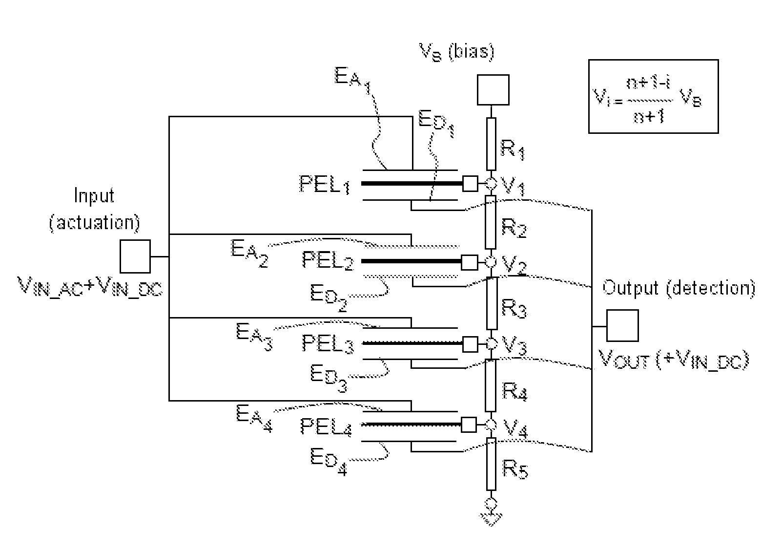
[0094]According to this example, which is illustrated in FIG. 7, the beams are cantilever beams i.e. beams that are fixed only at one of their ends and not fixed at both their ends as in the example illustrated in FIG. 6. FIG. 7 schematically shows one example with 4 beams PEL1, PEL2, PEL3 and PEL4, coupled to 4 actuation electrodes EA1, EA2, EA3 and EA4; FIG. 7 also shows elements R1, R2, R3, R4 and R5 (corresponding to resistors present between the various nodes of potentials Vi) and the potentials along the series of said cantilever beams mounted in series. By way of output, 4 electrodes ED1, ED2, ED3 and ED4 dedicated to detection are connected to a common output potential, the AC portion of which is VOUT (the detection signal), the DC portion advantageously being fixed at VIN—DC (in order to equalize the DC voltage exerted by the two types of electrodes on the beam).

[0095]Example of Implementation of the Invention with a Network of Plate R...


PUM


Abstract

A MEMS/NEMS device having an adjustable frequency response comprises an array of electrostatically actuated resonators, an electrostatic actuation circuit, electrical detection means, and means adjusting the frequency response of the resonators. The device comprises resonators having a movable portion, electrically connected in series between a first biasing potential VB and a second biasing potential VB2, each resonator biased to a potential Vi between VB and VB2, depending on position in the series. The electrostatic actuation circuit comprises, for each resonator, an actuation electrode facing the movable portion, all electrodes being connected in parallel to a common control potential VIN, the actuation voltage of each resonator being equal to VIN−Vi. The detection means comprises a detection output common to all resonators, the output being connected to an output potential Vout. The means for adjusting the frequency response varies the common control potential and/or at least one of the biasing potentials.

Description

CROSS-REFERENCE TO RELATED APPLICATION[0001]This application claims priority to foreign French patent application No. FR 1360855, filed on Nov. 6, 2013, the disclosure of which is incorporated by reference in its entirety.FIELD OF THE INVENTION[0002]The field of the invention is that of radio-frequency components (for filtering in particular) and notably that of sensors based on resonators (applied to sensors of variations in resonant frequency such as mass or gas sensors in particular).BACKGROUND[0003]Generally, the microsystems designated MEMS and / or NEMS, for micro and / or nanoelectromechanical systems, are components fabricated by means of microelectronics fabrication processes and certain dimensions of which may range from a few tens of nanometres to a few hundred microns.[0004]A great deal of research has been carried out on these components because they allow functionalities (sensors or actuators) to be obtained that were difficult to obtain with “conventional” microelectronic...

Claims


Application Information

Patent Timeline
Patent Type & Authority Applications(United States)
IPC IPC(8): H03H9/02H03H9/46
CPCH03H9/02259H03H2009/02291H03H9/462H03H9/02393H03H9/525
Inventor ARCAMONE, JULIENARNDT, GREGORY
Owner COMMISSARIAT A LENERGIE ATOMIQUE ET AUX ENERGIES ALTERNATIVES
Why Eureka
Try Eureka