

Method of wafer-scale integration of semiconductor devices and semiconductor device
- Summary
- Abstract
- Description
- Claims
- Application Information
AI Technical Summary
Benefits of technology
Problems solved by technology
Method used
Image

Examples
Embodiment Construction
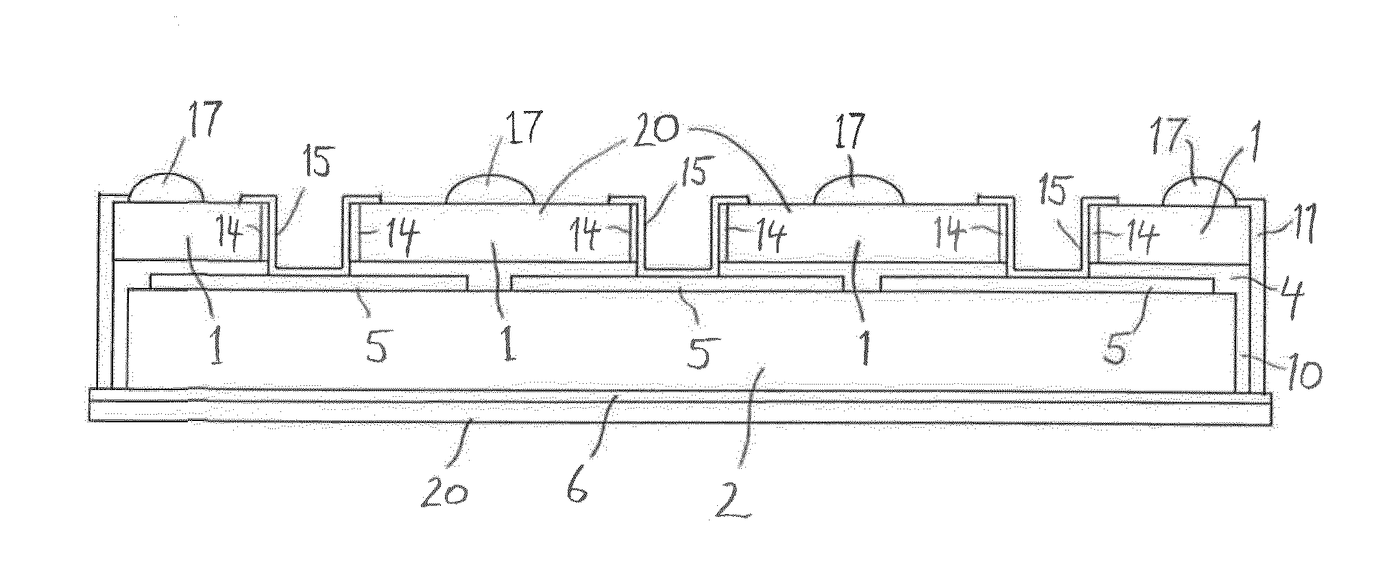
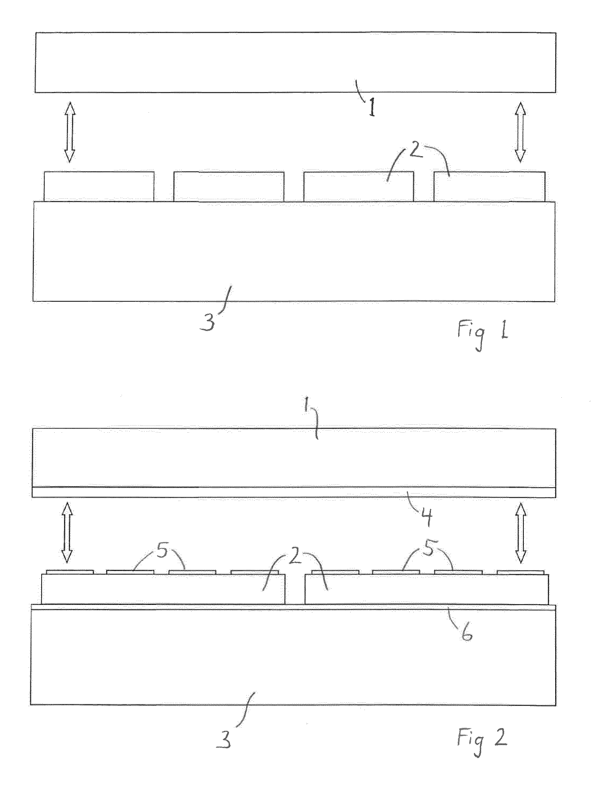
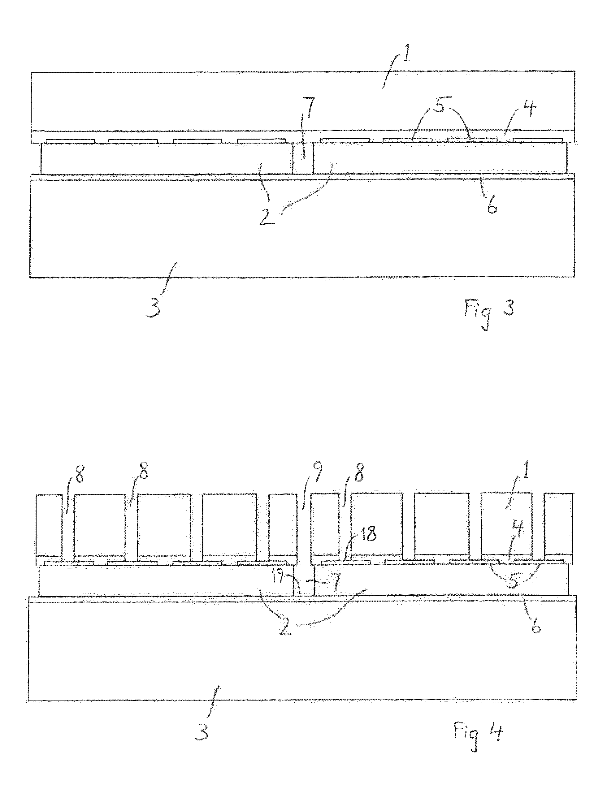
[0026]FIG. 1 shows a cross section of an arrangement of a semiconductor wafer 1, a further semiconductor wafer 2, which differs from the first semiconductor wafer 1 in its size, in its material or in its size and material, and a handling wafer 3. The further semiconductor wafer 2 is fastened to the handling wafer 3. In the embodiment shown in FIG. 1 the further semiconductor wafer 2 has before been divided into dies, which may have been done by any usual method of wafer dicing. The dies may be selected to secure that only “known good dies” are used. The dies are arranged on the handling wafer 3 and permanently fastened to the handling wafer 3. The further semiconductor wafer 2 may instead be one piece only, or it may be separated into dies after having been fastened to the handling wafer 3. The arrangement of the further semiconductor wafer 2 and the handling wafer 3 is then bonded to the semiconductor wafer 1. For this purpose the semiconductor wafer 1 may be provided with a bondin...
PUM
 Abstract
Description
Claims
Application Information