Organic light emitting display device and method of manufacturing the same

a technology of light-emitting display device and which is applied in the direction of thermoelectric device junction material, semiconductor device, electrical apparatus, etc., can solve the problems of cracks generated on the bonding surface, spread to the entire substrate, and degraded organic light-emitting display device, so as to achieve effective blocking of ambient oxygen and moisture and increase mechanical strength

Inactive Publication Date: 2015-05-28
SAMSUNG DISPLAY CO LTD
View PDF11 Cites 14 Cited by
  • Summary
  • Abstract
  • Description
  • Claims
  • Application Information

AI Technical Summary

Benefits of technology

[0010]An embodiment of the present invention relates to an organic light emitting display device and a method of manufacturing the same, capable of increasing mechanical strength and effectively blocking ambient oxygen and moisture.
[0012]An organic light emitting display device according to an embodiment of the present invention includes: a substrate having at least one thin film transistor (TFT); an organic light emitting element having a first electrode electrically connected to the TFT, a pixel defining layer formed on the first electrode and having an opening partially exposing the first electrode, an organic emission layer formed on the first electrode, and a second electrode formed on the organic emission layer; a sealing unit sealing the organic light emitting element along the edges of the substrate; and a reinforcing unit positioned within a hole partially formed in the pixel defining layer and enhancing strength of the substrate.

Problems solved by technology

However, organic light emitting display devices have characteristics of being degraded by ambient oxygen and moisture infiltration.
Meanwhile, due to the brittleness of the frit material used in the frit encapsulation structure, when external impact is applied, stress is concentrated on a bonding surface between the frit and the substrate to cause cracks to be generated in the bonding surface and spread to the entire substrate.

Method used


Image

  • Organic light emitting display device and method of manufacturing the same
  • Organic light emitting display device and method of manufacturing the same
  • Organic light emitting display device and method of manufacturing the same

Examples


Embodiment Construction

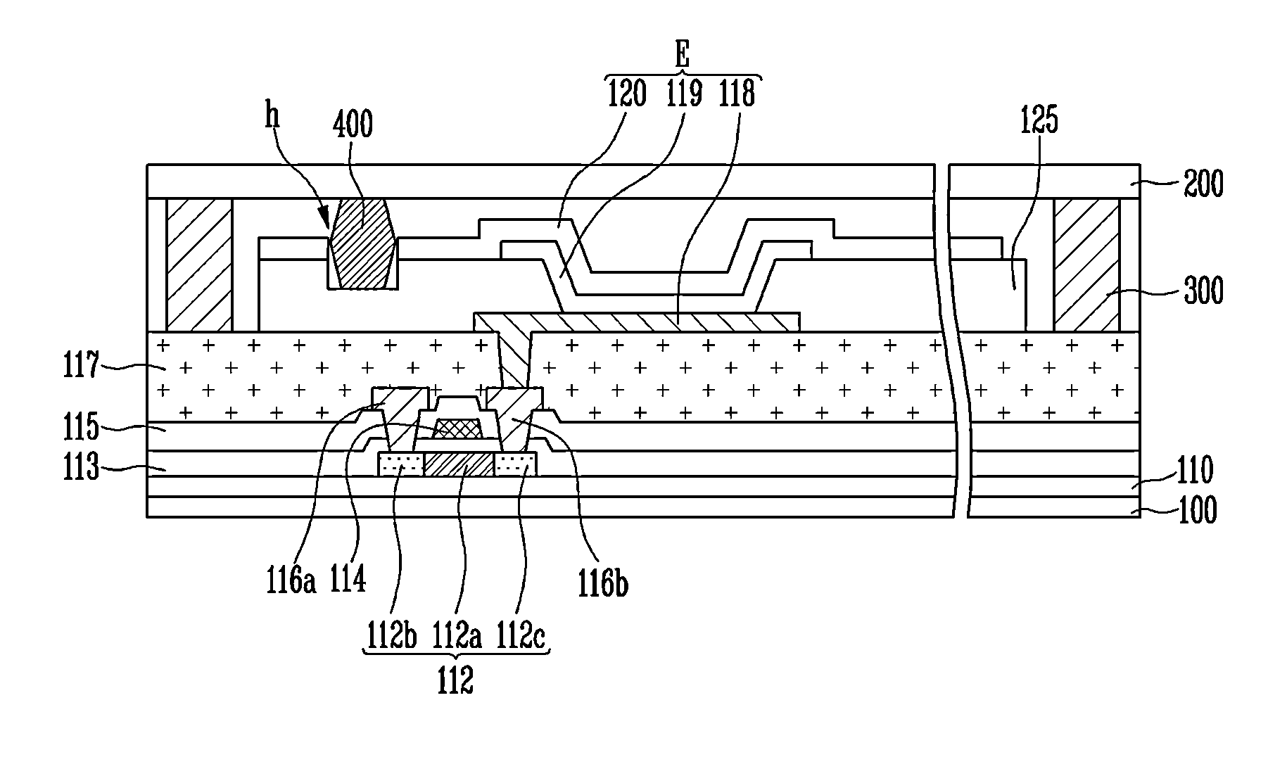
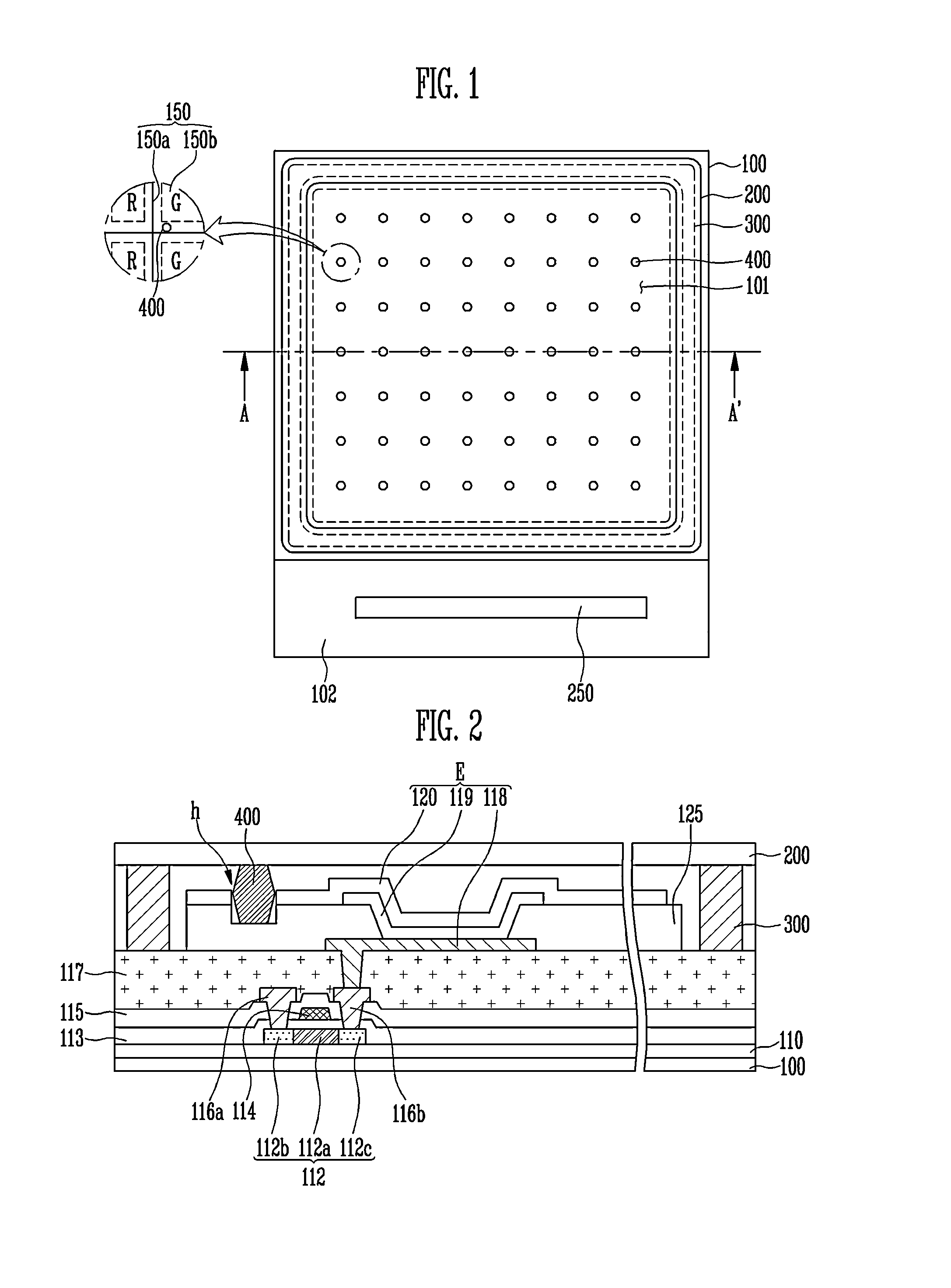
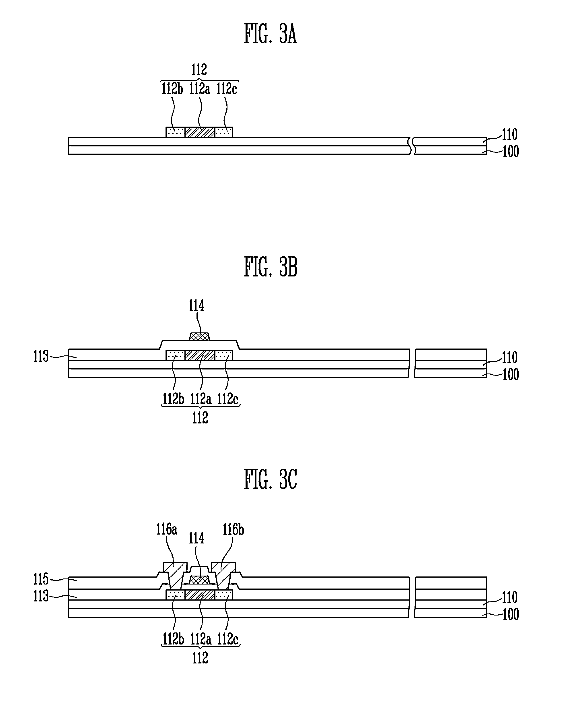
[0034]Details of embodiments are included in detailed descriptions and drawings.

[0035]The advantages and features of the present disclosure and methods for achieving these will be clarified in detail through embodiments described hereinafter in conjunction with the accompanying drawings.

[0036]However, embodiments of the present invention may, however, be implemented in many different forms and should not be construed as being limited to the embodiments set forth herein. Rather, these embodiments are provided so that this disclosure will be thorough and complete, and will fully convey the scope of the invention to those skilled in the art and are defined by the claim coverage of the present invention. Throughout the specification, the same reference numerals will be used to designate the same or like components.

[0037]In order to clarify the present invention, parts that are not connected with the description will be omitted, and since sizes and thickness of respective components are ...


PUM


Abstract

An organic light emitting display device includes a first substrate, a second substrate, and an array of organic light emitting elements formed over the first substrate and interposed between the first and second substrate. The array comprises a pixel defining layer. The organic light emitting display device further includes a recess formed into the pixel defining layer, a sealing member, and a reinforcing member. The sealing member is formed along the edges of the first and second substrates and interconnects the first and second substrates. The reinforcing member comprises a first portion positioned in the recess and a second portion projected outside the recess toward the second substrate such that the second portion of the reinforcing member is capable of supporting the second substrate when the second substrate is pressed toward the first substrate by an external force.

Description

CROSS-REFERENCE TO RELATED APPLICATION[0001]This application claims priority to and the benefit of Korean Patent Application No. 10-2013-0142584, filed on Nov. 22, 2013, in the Korean Intellectual Property Office, the entire contents of which are incorporated herein by reference in their entirety.BACKGROUND[0002]1. Field[0003]The present disclosure relates to an organic light emitting display device and a method of manufacturing the same.[0004]2. Description of the Related Art[0005]An organic light emitting display device a flat panel display device in which an organic emission layer is positioned between electrodes facing each other. Electrons injected from one electrode and holes injected from the other electrode are combined in the organic emission layer to excite luminescent molecules of the organic emission layer, and as the excited molecules are subsequently returned to a ground state, energy is released to emit light.[0006]Because organic light emitting display devices have e...

Claims


Application Information

Patent Timeline
Patent Type & Authority Applications(United States)
IPC IPC(8): H01L27/32H01L51/52H01L51/56
CPCH01L27/3253H01L51/56H01L2227/323H01L27/3246H01L51/5246H10K59/122H10K50/8428H10K50/8426H10K59/1201H10K50/841H10K50/84
Inventor KOO, YONG-KYOUNGKIM, KWANG-SEONG
Owner SAMSUNG DISPLAY CO LTD
Why Eureka
Try Eureka