
Eureka
For R&D, Eureka makes reading and utilizing patents & technical documents easy.
Eureka AIR
Designed for self-driven R&D workflows. Generate viable solutions, solve complex R&D challenges, empower your innovation with AI.

Eureka Materials
Designed for material experts only. Revolutionize your material R&D, from search, analyze, to developing new materials.

TechResearch
Generate reliable direction feasibility study reports for your R&D in just a few steps.

TechSeek
Discover and master advanced knowledge NOW. Basics, ideas, possibilities, all at once.

TechMind
As an expert in R&D Theories, TechMind can generates customized viable solutions instantly.

TechRisk
Analyze your overall solution with one click, know your potential R&D risks in advance.

TechMonitor
Get weekly tech updates, stay abreast of the latest tech innovations and key insights.
Display substrate and method of manufacturing the same
- Summary
- Abstract
- Description
- Claims
- Application Information
AI Technical Summary
Benefits of technology
Problems solved by technology
Method used
Image

Examples
Embodiment Construction
[0034]Hereinafter, example embodiments will be explained in detail with reference to the accompanying drawings.
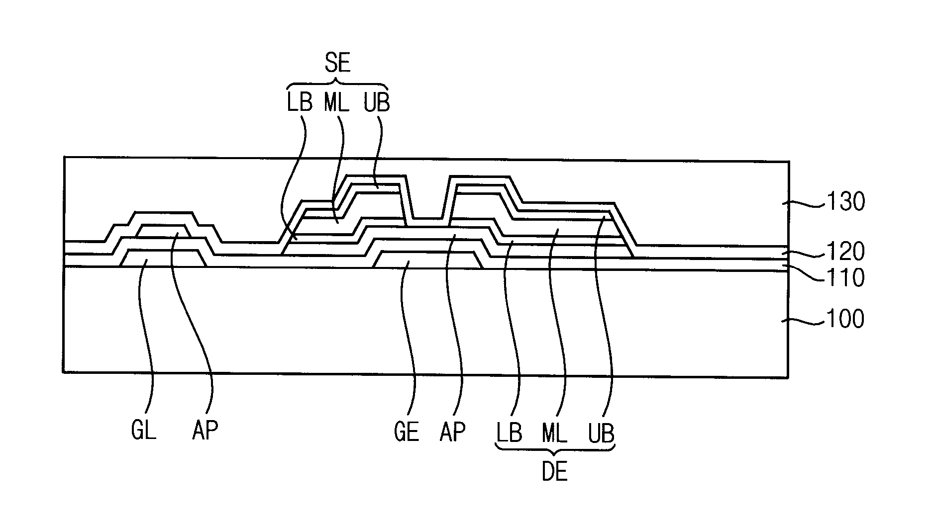
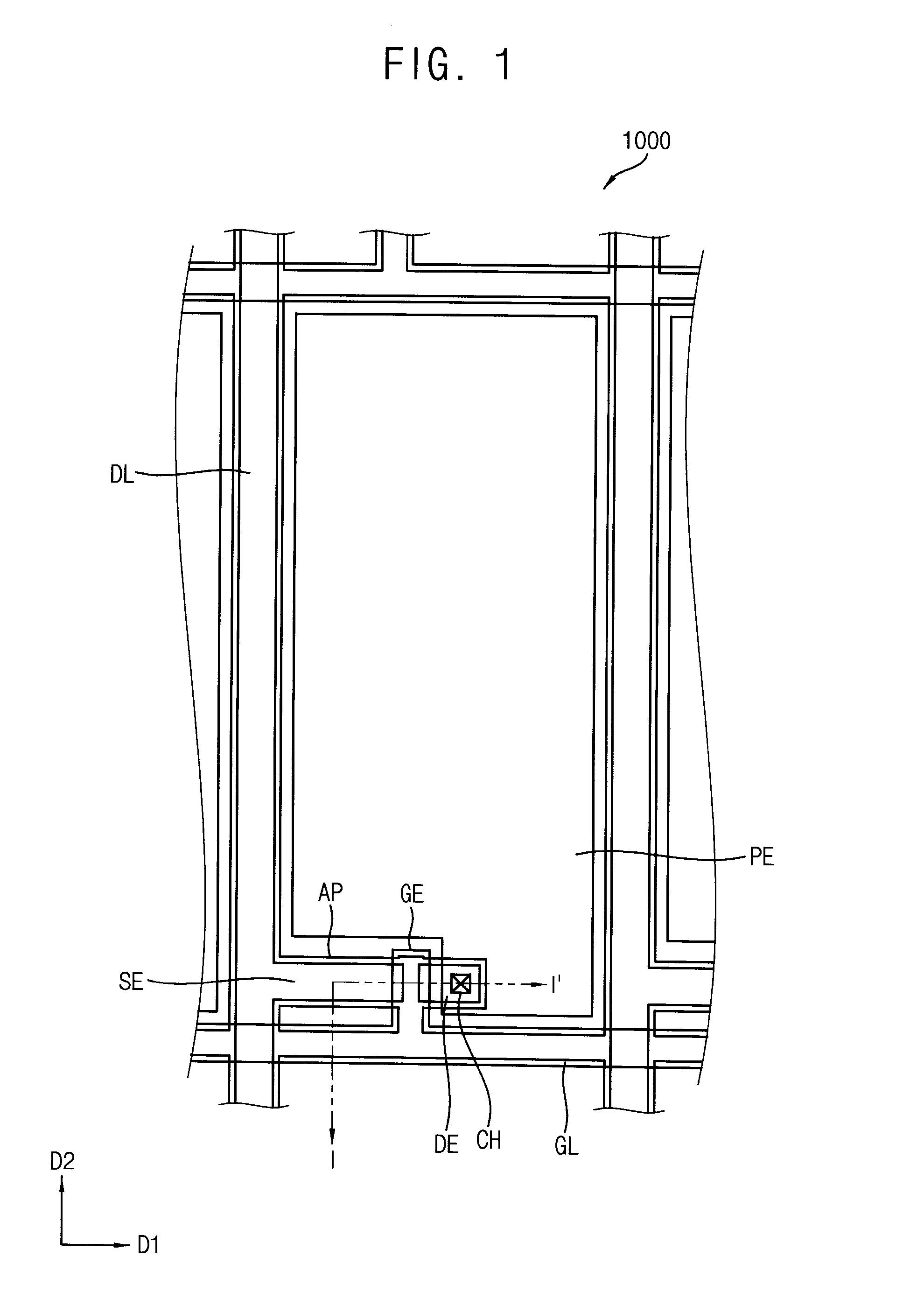
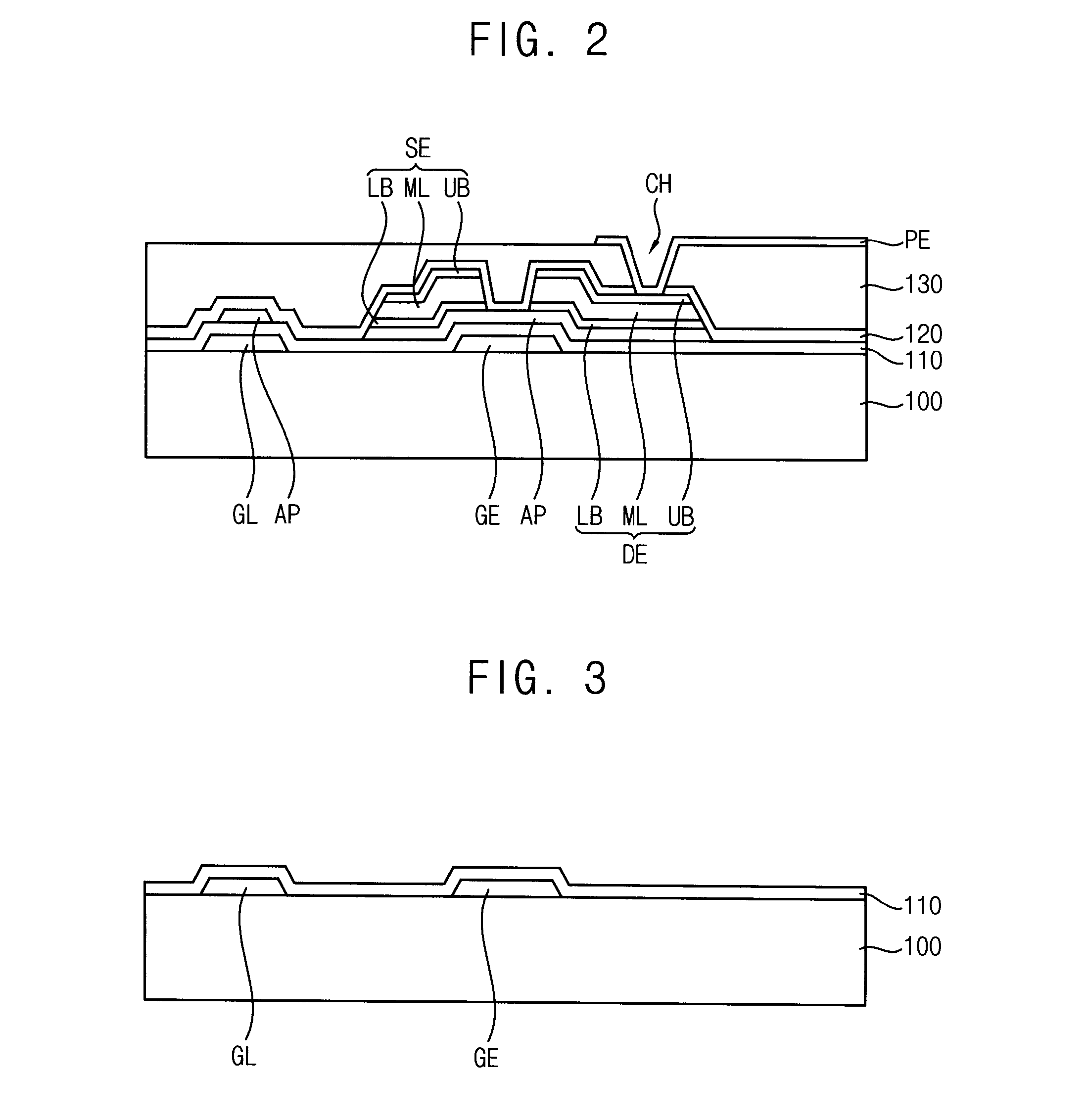
[0035]FIG. 1 is a plan view illustrating a display substrate according to an example embodiment. FIG. 2 is a cross-sectional view taken along the line I-I′ of FIG. 1.
[0036]Referring to FIGS. 1 and 2, a display substrate includes a base substrate 100, a gate line GL, a data line DL, a gate insulation layer 110, a thin film transistor, a passivation layer 120, an organic insulation layer 130 and a pixel electrode PE. The thin film transistor includes a gate electrode GE, an active pattern AP, a source electrode SE and a drain electrode DE.
[0037]The gate line GL extends along a first direction D1. The data line DL extends along a second direction D2 substantially perpendicular to the first direction D1, and crosses the gate line GL.
[0038]The gate line GL and the data line DL define a pixel area. Although only one pixel area is generally described in the figures, the display su...
PUM
 Abstract
Description
Claims
Application Information
 - R&D Engineer
- R&D Manager
- IP Professional
- Industry Leading Data Capabilities
- Powerful AI technology
- Patent DNA Extraction
Browse by: Latest US Patents, China's latest patents, Technical Efficacy Thesaurus, Application Domain, Technology Topic, Popular Technical Reports.
© 2024 PatSnap. All rights reserved.Legal|Privacy policy|Modern Slavery Act Transparency Statement|Sitemap|About US| Contact US: help@patsnap.com