Reactor for plasma-based atomic layer etching of materials

a technology of atomic layer etching and plasma, which is applied in the direction of coatings, chemical vapor deposition coatings, electric discharge tubes, etc., can solve the problems of insignificant physical sputtering of unmodified materials after etching, and inability to achieve self-limited etching

Active Publication Date: 2015-06-11
UNIV OF MARYLAND
View PDF5 Cites 350 Cited by
  • Summary
  • Abstract
  • Description
  • Claims
  • Application Information

AI Technical Summary

Benefits of technology

[0009]According to certain embodiments, an apparatus may include a coupled plasma system containing a chemical precursor to be energized by the plasma and deposited on a substrate. The apparatus may also include a power source configured to supply a radio frequency bias potential to the substrate. The apparatus may further include a controller configured to control an amount of the chemical precursor applied to the substrate to create a chemical precursor layer

Problems solved by technology

These efforts have shown that a key obstacle toward realizing ALE is achieving self-limited etching, in particular for situations when ion bombardment to remove the reacted material and precise control of surface coverage by the chemical p

Method used


Image

  • Reactor for plasma-based atomic layer etching of materials
  • Reactor for plasma-based atomic layer etching of materials
  • Reactor for plasma-based atomic layer etching of materials

Examples


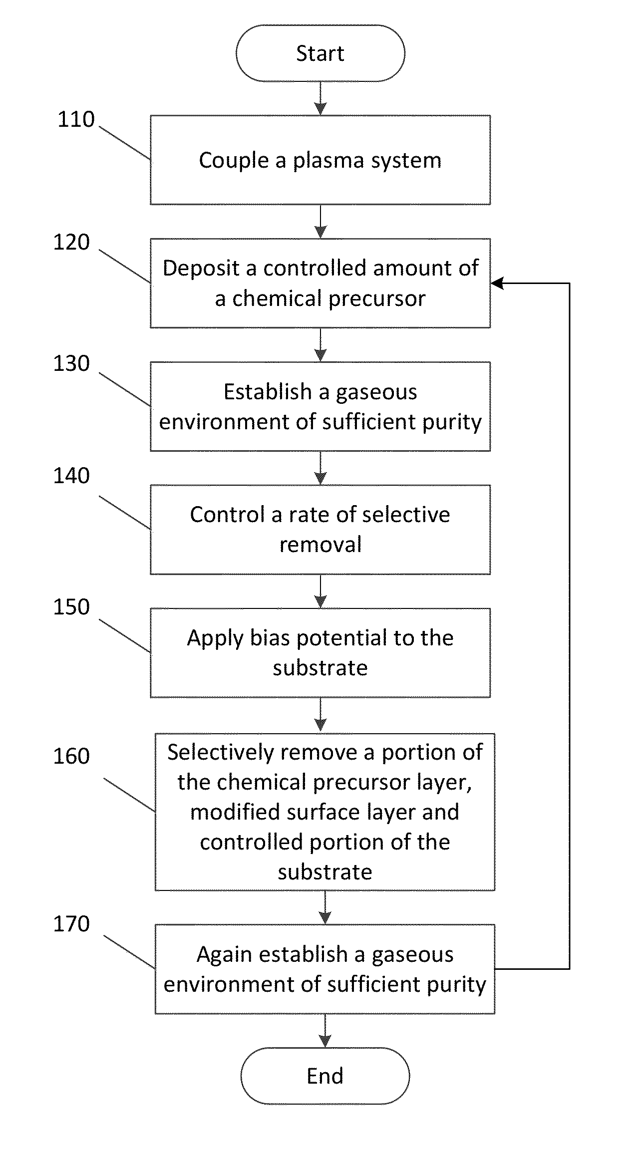
Embodiment Construction

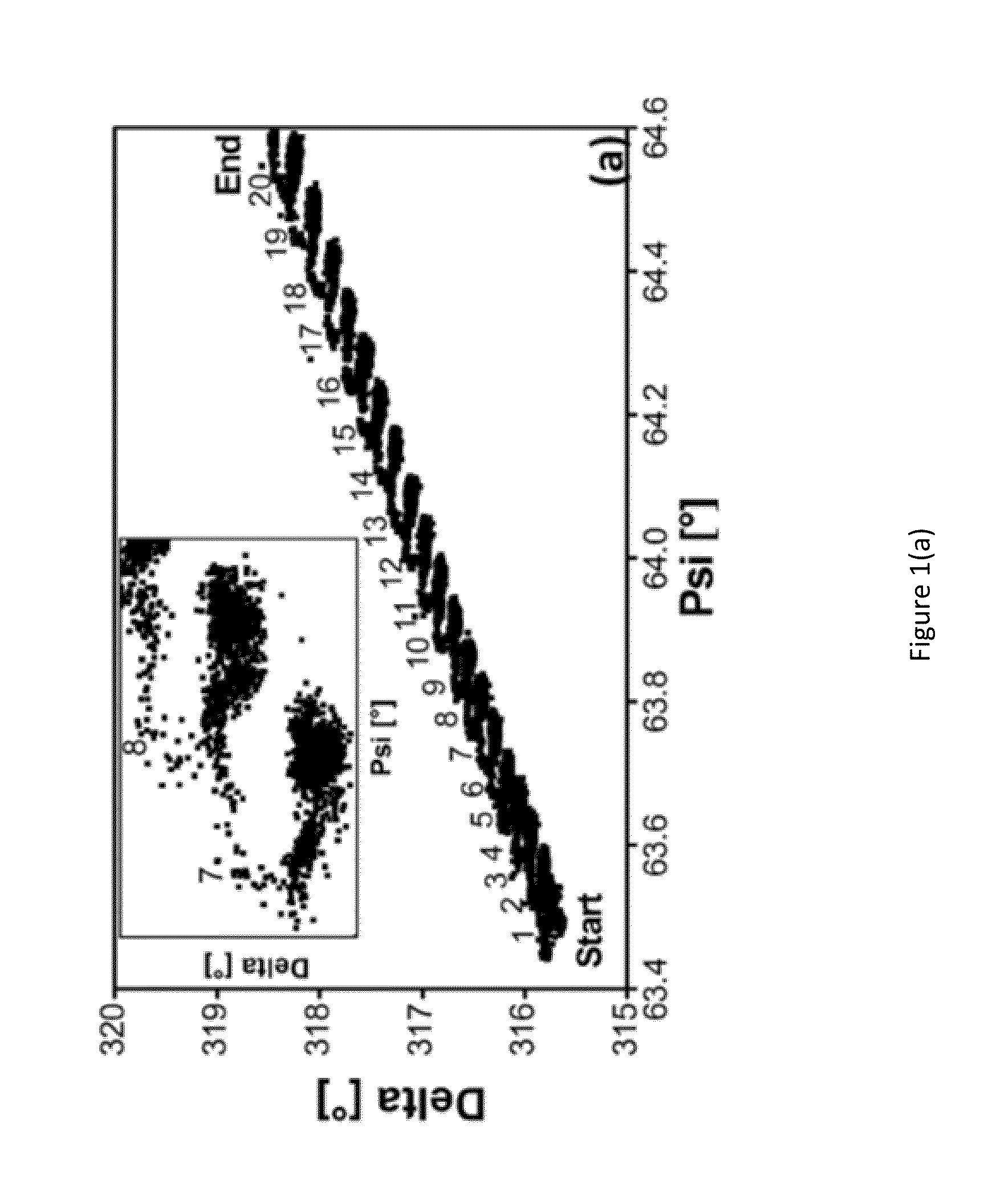
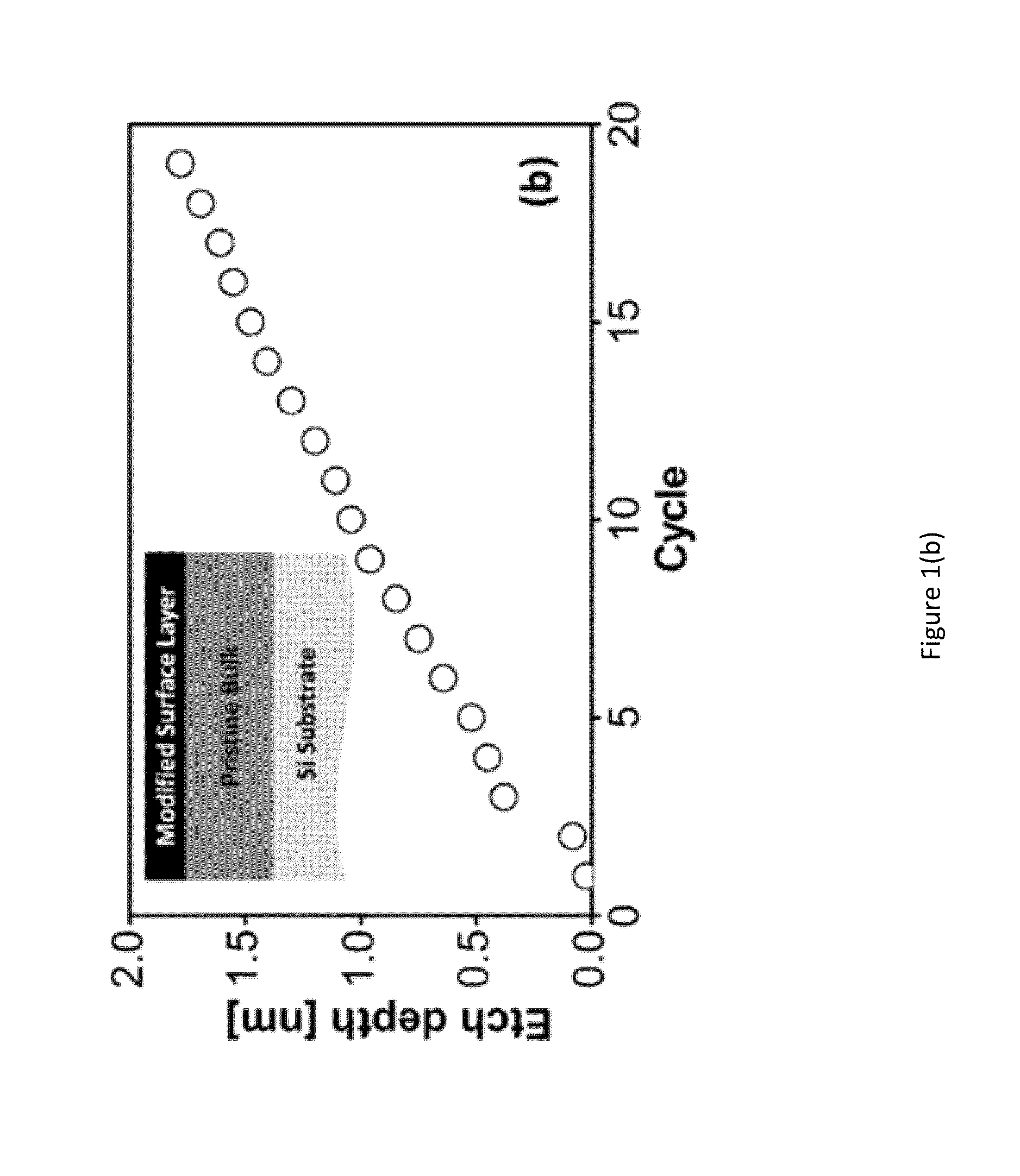
[0030]According to certain embodiments, it may be possible to study and evaluate the use of cyclic plasma interacting with a substrate. For example, cyclic Ar / C4F8 plasma interacting with a substrate can be explored to determine for what conditions controlled removal of substrate layers approaching one atomic layer thickness per cycle can be achieved. Conditions for the removal of substrate layers ranging from about 1 / 10 of an angstrom to about 1 nm can be achieved. In other embodiments, time-resolved surface characterization can be implemented to confirm ALE.

[0031]The term atomic layer etching, as used herein, can broadly refer to the level of layer dimensional control that can be achieved at the angstrom level. Thus, atomic layer etching may generally correspond to the size of atoms. Additionally, the average removed layer thickness / cycle can be less than 1 angstrom per etching cycle, or more than 1 angstrom / cycle.

[0032]Various substrates may be used in studying and evaluating the...


PUM

PropertyMeasurementUnit
Thicknessaaaaaaaaaa
Thicknessaaaaaaaaaa
Thicknessaaaaaaaaaa

Abstract

Plasma-based atomic layer etching of materials may be of benefit to various semiconductor manufacturing and related technologies. For example, plasma-based atomic layer etching of materials may be beneficial for adding and/or removing angstrom thick layers from a surface in advanced semiconductor manufacturing and related technologies that increasingly demand atomistic surface engineering. A method may include depositing a controlled amount of a chemical precursor on an unmodified surface layer of a substrate to create a chemical precursor layer and a modified surface layer. The method may also include selectively removing a portion of the chemical precursor layer, a portion of the modified surface layer and a controlled portion of the substrate. Further, the controlled portion may be removed to a depth ranging from about 1/10 of an angstrom to about 1 nm. Additionally, the deposition and selective removal may be performed under a plasma environment.

Description

CROSS-REFERENCE TO RELATED APPLICATIONS[0001]This application is related to and claims the benefit and priority of U.S. Provisional Patent Application No. 61 / 913,013, filed Dec. 6, 2013, which is hereby incorporated by reference in its entirety.BACKGROUND[0002]1. Field[0003]Plasma-based atomic layer etching of materials may be of benefit to various semiconductor manufacturing and related technologies. For example, plasma-based atomic layer etching of materials may be beneficial for removing angstrom thick layers from a surface in advanced semiconductor manufacturing and related technologies that increasingly demand atomistic surface engineering.[0004]2. Description of the Related Art[0005]While atomic layer deposition has been tremendously successful, the development of a corresponding atomic layer etching (ALE) method has lagged. In atomic layer deposition, control of deposited film thickness near one atomic monolayer may be based on careful choice of chemical precursors which, onc...

Claims


Application Information

Patent Timeline
IPC IPC(8): H01J37/32H01L21/311C23C16/455C23C16/56C23C16/52
CPCH01J37/32091H01J37/321H01J37/32146C23C16/56C23C16/52H01J2237/334C23C16/45544H01L21/31116H01L21/31122H01J2237/3321C23C16/45536H01J37/32082
Inventor OEHRLEIN, GOTTLIEB S.METZLER, DOMINIK
Owner UNIV OF MARYLAND
Why Eureka
Try Eureka