Integrated circuits with dummy contacts and methods for producing such integrated circuits

a technology of integrated circuits and contacts, which is applied in the direction of electrical equipment, semiconductor devices, semiconductor/solid-state device details, etc., can solve the problems of under-sized vias in crowded areas, and achieve the effect of reducing the variation in contact density

Inactive Publication Date: 2015-06-18
GLOBALFOUNDRIES SINGAPORE PTE LTD
View PDF1 Cites 174 Cited by
  • Summary
  • Abstract
  • Description
  • Claims
  • Application Information

AI Technical Summary

Benefits of technology

[0006]In another exemplary embodiment, a method for fabricating an integrated circuit includes forming an interlayer dielectric overlying an electronic components and a substrate, wherein the interlayer dielectric has an interlayer dielectric top surface. The interlayer dielectric top surface is divided into a plurality of regions including a first region and a second region. An active contact is formed within the interlayer dielectric, where the active contacts extend through the interlayer dielectric and forms an electrical connection with the electronic component, and where there are more active contacts in the first region than in the second region. A contact density variation is decreased by forming a dummy contact within the interlayer dielectric in the second region.

Problems solved by technology

If the via is too small, the contact will not make an electrical connection with the electronic component, and if the via is too large the contact will form a “short” and make an unwanted electrical connection to an adjacent contact area and thereby cause a failure.
Therefore, vias tend to be undersized in crowded areas, and oversized in areas where relatively few vias are etched.

Method used


Image

  • Integrated circuits with dummy contacts and methods for producing such integrated circuits
  • Integrated circuits with dummy contacts and methods for producing such integrated circuits
  • Integrated circuits with dummy contacts and methods for producing such integrated circuits

Examples


Embodiment Construction

[0011]The following detailed description is merely exemplary in nature and is not intended to limit the application and uses of the embodiment described. Furthermore, there is no intention to be bound by any theory presented in the preceding background or the following detailed description.

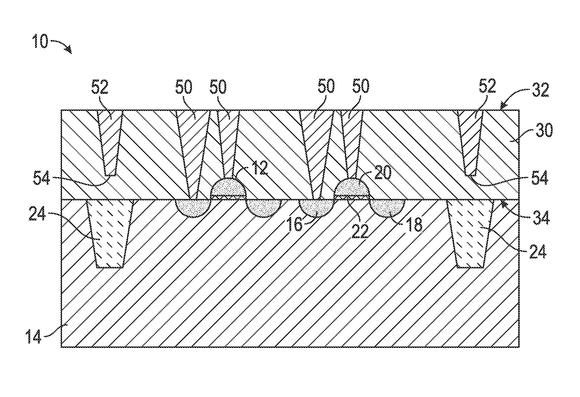
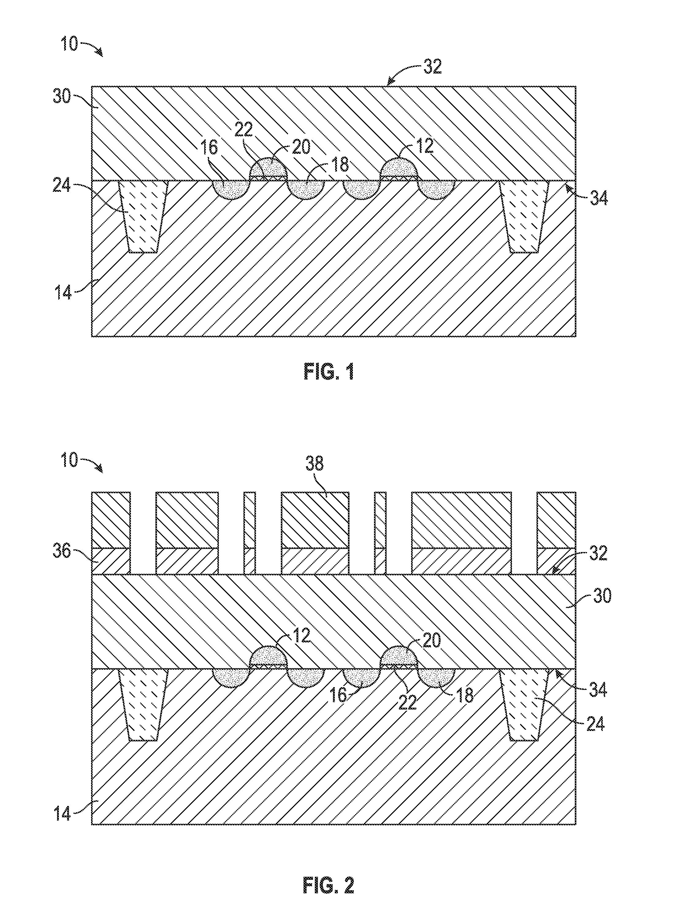
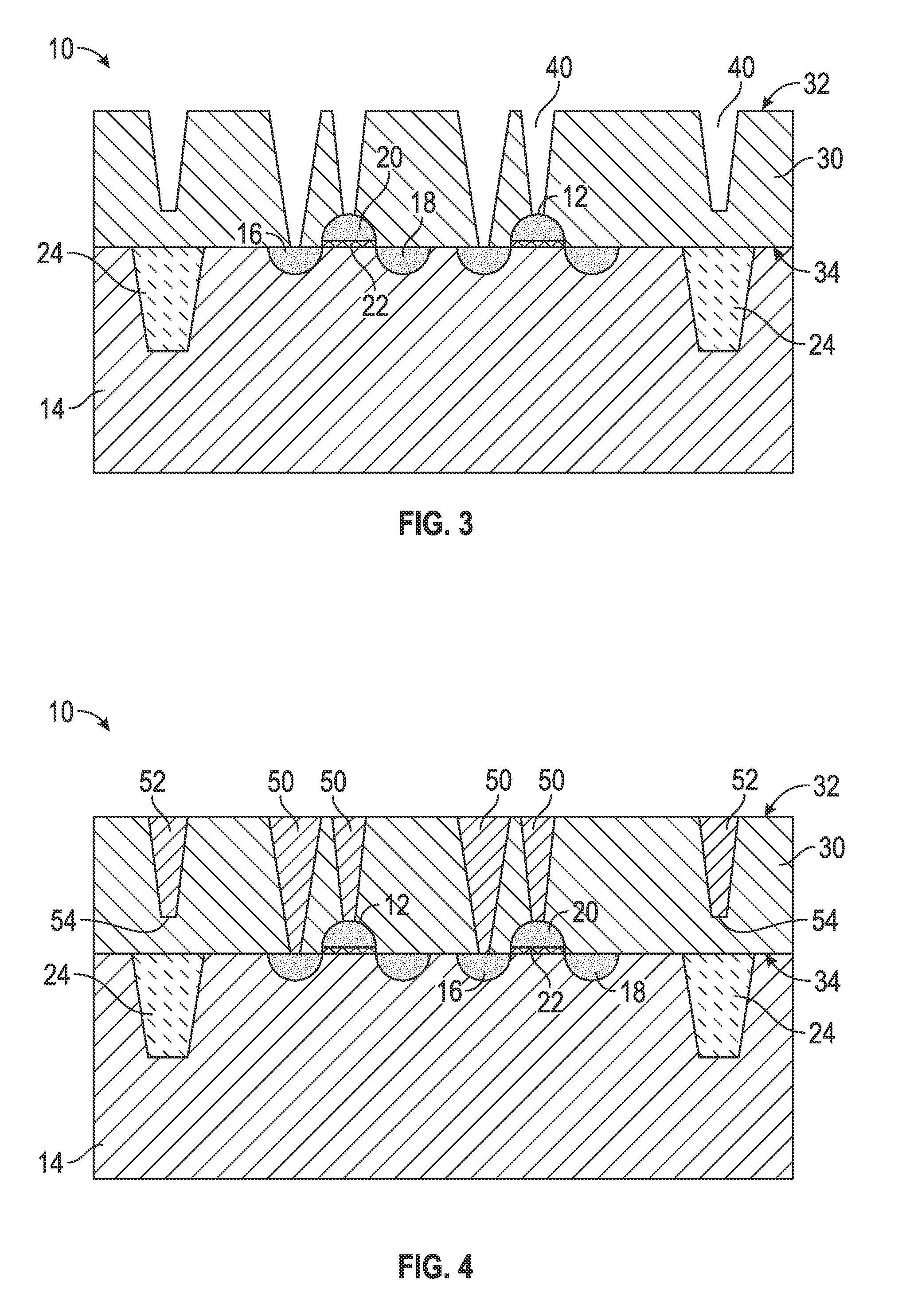
[0012]Integrated circuits include many contacts that extend through an interlayer dielectric to make electrical contact with an electronic component under the interlayer dielectric. In some embodiments, the contacts are formed by anisotropically etching a via through the interlayer dielectric, and filling the via with a conductive material to form the contact. A plasma is used to etch the vias, and the etch rate of the plasma varies with the amount of material being etched locally. Therefore, a region with many vias will tend to have a slower etch rate than a region without many vias. The variation in the etch rate increases the variation in the contact size, which increases manufacturing toleranc...


PUM


Abstract

Integrated circuits with dummy contacts and methods for fabricating such integrated circuits are provided. The method includes forming an interlayer dielectric overlying an electronic component and a substrate, wherein the interlayer dielectric has an interlayer dielectric top surface. An active contact is formed through the interlayer dielectric and forms an electrical connection with the electronic component. A dummy contact is formed within the interlayer dielectric where the dummy contact extends to a dummy contact termination point between the interlayer dielectric top surface and the substrate such that an insulator is positioned between the dummy contact termination point and the electronic component.

Description

TECHNICAL FIELD[0001]The technical field generally relates to integrated circuits and methods for producing integrated circuits, and more particularly relates to integrated circuits with dummy contacts and methods for producing such integrated circuits.BACKGROUND[0002]Over time, integrated circuits are becoming smaller but with increased capabilities. The production of smaller integrated circuits requires the development of smaller electronic components, and closer spacing of those electronic components. In traditional integrated circuits, contacts are formed through an insulating cover layer, often called an interlayer dielectric, to form electrical connections with the underlying electronic components. Interconnects or metallization layers are then formed overlying the interlayer dielectric, where the interconnects electrically connect the electronic components in a desired manner by forming electrical connections with the contacts. There may be several layers of interconnect line...

Claims


Application Information

Patent Timeline
Patent Type & Authority Applications(United States)
IPC IPC(8): H01L23/522H01L21/768H01L21/311H01L23/532H01L21/02
CPCH01L23/5226H01L23/53228H01L23/53257H01L21/76877H01L21/02164H01L21/31116H01L21/76802H01L23/5329H01L23/485H01L23/53238H01L23/53266H01L2924/0002H01L21/76816H01L2924/00
Inventor LUO, LAIQIANGLIANG, JIANFANGCHEN, AARONCHANG, TIAN-LINZHANG, FANTAN, JUAN BOON
Owner GLOBALFOUNDRIES SINGAPORE PTE LTD
Why Eureka
Try Eureka