
Micro-led array with filters

Active Publication Date: 2015-06-25
META PLATFORMS TECH LLC
View PDF5 Cites 20 Cited by
  • Summary
  • Abstract
  • Description
  • Claims
  • Application Information

AI Technical Summary

Benefits of technology

The LED device is designed to emit light that is almost completely parallel to the surface it is emitting from, which makes it easier for the light to be directed by the optical component. This arrangement allows for the optical component to be placed directly on the surface of the LED device, resulting in an integrated LED device that doesn't require any additional optical components. Overall, this technology helps improve the efficacy of the LED device and makes it more efficient in producing light.

Problems solved by technology

A major challenge is to extract as much of the emitted light as possible from the semiconductor material into the surrounding medium, typically air.
Long path lengths and reflections at metal coated semiconductor surfaces both lead to absorption losses.
However, it does not eliminate the long path lengths within the semiconductor chip, nor the requirement for an external mirror.
Also, the technique is less suitable to the widely used gallium nitride (GaN) based materials systems.
The reason for this is that the sapphire and silicon carbide (SiC) substrates commonly used in GaN-based LED-chips are both very hard materials and very difficult to shape mechanically, for example with a dicing saw.
In LED devices using such materials, it seems not to be a practical solution to shape the whole chip.
Therefore, additional components are typically required for the correct operation of an LED device, but they add bulk and complexity to the device itself and the optical path of the light within the device before it escapes from the light emitting surface.

Method used


Image

  • Micro-led array with filters
  • Micro-led array with filters
  • Micro-led array with filters

Examples


Embodiment Construction

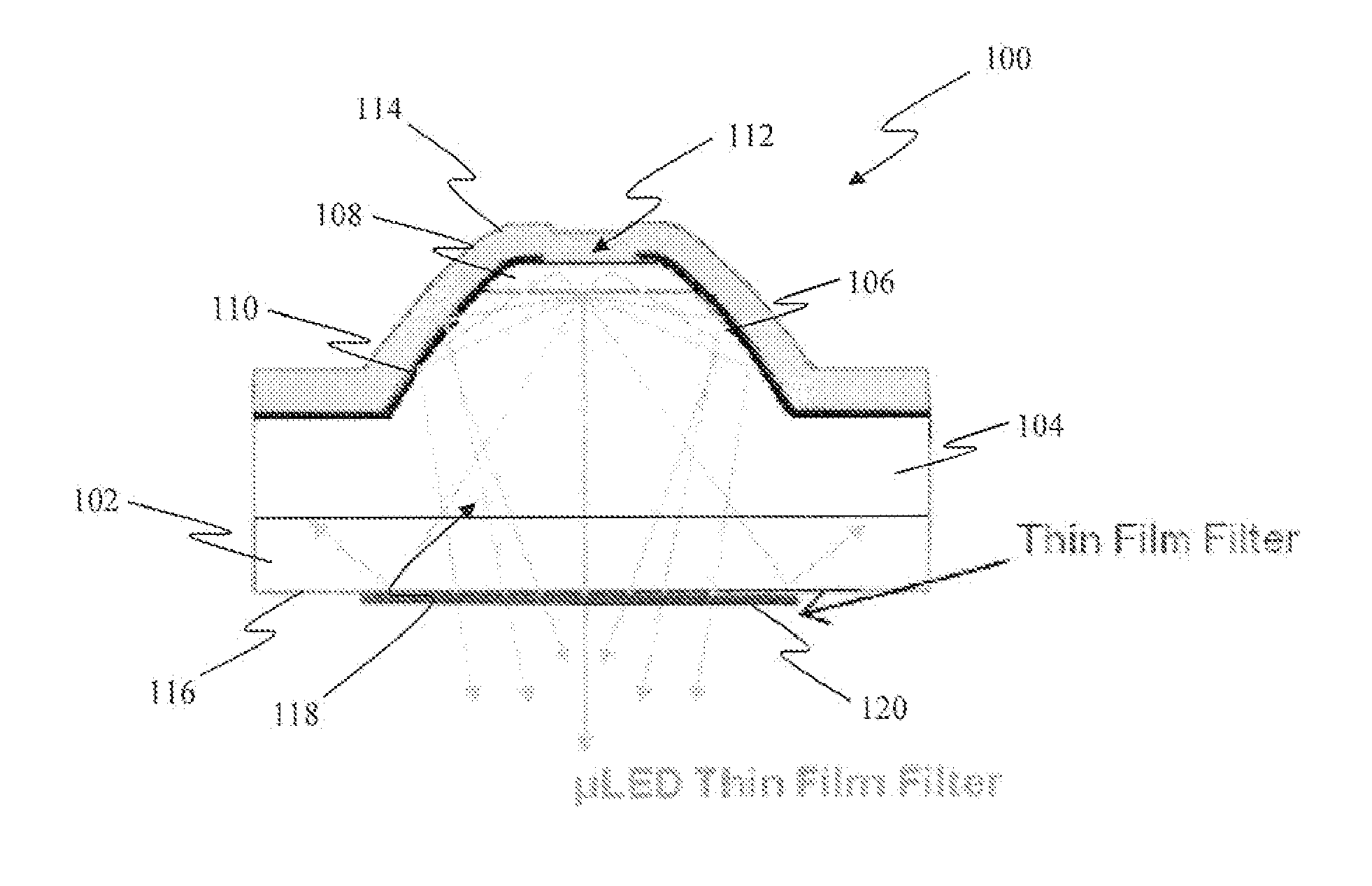
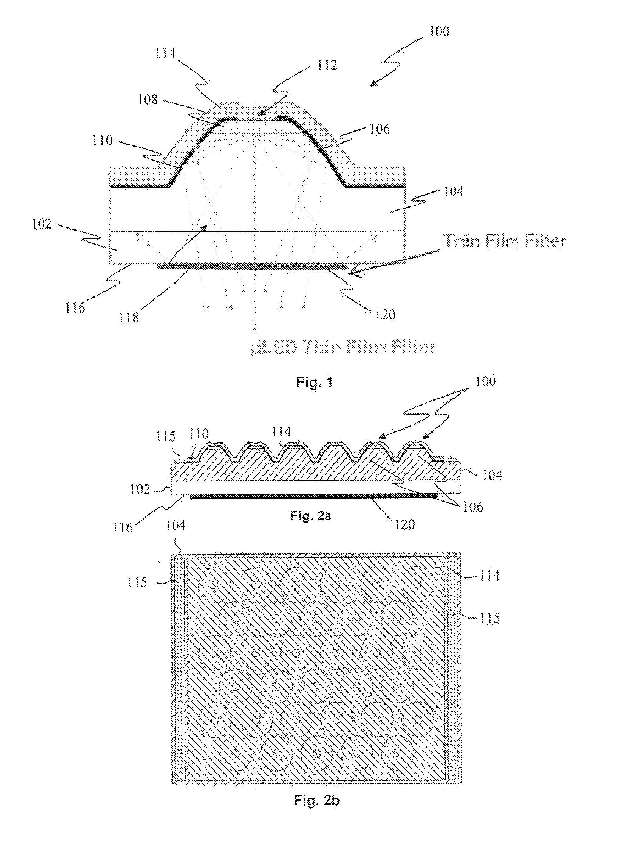
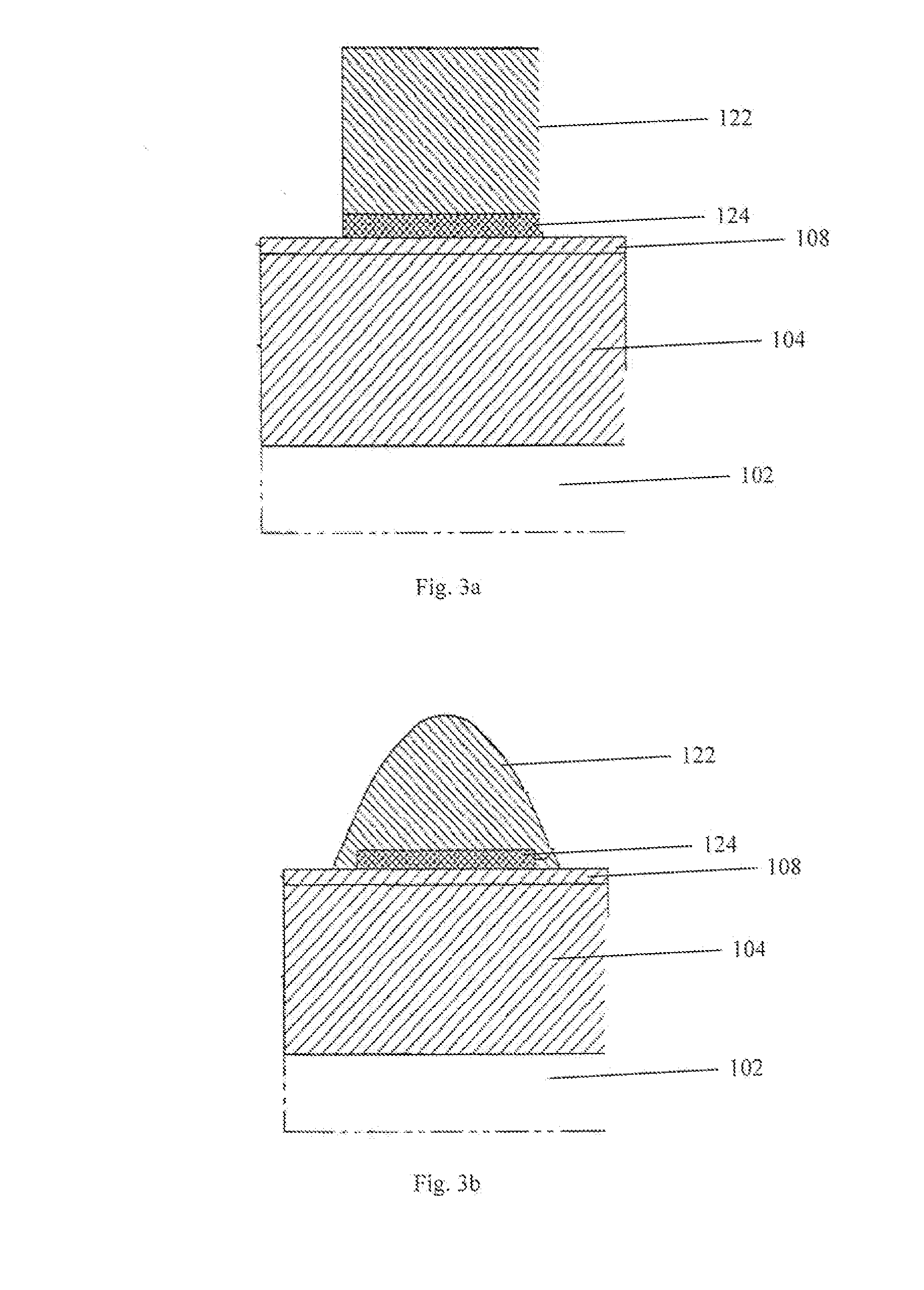
[0037]Generally, disclosed herein is an LED device having an optical component integrated into the device and configured to change an optical property of at least some of the light emitted from the device. In exemplary LED devices, the optical component is a coating applied to a light emitting surface of the device. Exemplary LED devices include a micro-LED (μLED) device with one or more optical coatings on a light emitting surface.

[0038]The surface where the light escapes from the LED may be referred to as the “light emitting surface”, the “light exiting surface”. Light is generated in a light generating layer, which may also be termed a light emitting layer, and the surface closest to this layer may be referred to as the light generating surface.

[0039]The inventors have appreciated that the performance of optical components is generally affected by the angle of incidence of light on the optical component. The inventors have further appreciated that an LED device may be configured ...


PUM


Abstract

An integrated LED device is provided. The LED device includes a substrate. The LED device includes a semiconductor material including a light generating layer and positioned on the substrate. The semiconductor material and / or the substrate are configured to control light internally to output quasi-collimated light from a light emitting surface of the LED device. The LED device includes an optical component positioned at the light emitting surface and configured to receive quasi-collimated light exiting the light emitting surface and to alter one or more optical properties of at least some beams of the quasi-collimated light.

Description

CROSS-REFERENCE TO RELATED APPLICATIONS[0001]This application is a National Phase Application filed under 35 USC 371 of International Application No. PCT / EP2013 / 053215, filed on Feb. 18, 2013, which claims the benefit and priority from U.S. Provisional Patent Application No. 61 / 599,731, filed Feb. 16, 2012, the disclosures of which are incorporated herein by reference in their entirety.TECHNICAL FIELD[0002]The present disclosure relates to LED devices, arrays of LED devices and methods of manufacturing LED devices. Specifically, the present disclosure relates to, but is not limited to, LED devices including an optical component located on a light emitting surface of the LED device. More specifically, the present disclosure relates to, but is not limited to, μLED devices providing a quasi-collimated light output.BACKGROUND OF THE INVENTION[0003]LEDs convert electrical energy into optical energy. In semiconductor LEDs, light is usually generated through recombination of electrons, ori...

Claims


Application Information

Patent Timeline
IPC IPC(8): H01L33/58H01L33/46H01L33/64H01L33/44
CPCH01L33/58H01L33/44H01L2933/0025H01L33/64H01L2933/0058H01L33/46H01L33/08H01L33/20
Inventor MAASKANT, PLEUNCORBETT, BRIANHENRY, BILL
Owner META PLATFORMS TECH LLC
Features
  • Generate Ideas
  • Intellectual Property
  • Life Sciences
  • Materials
  • Tech Scout
  • Unparalleled Data Quality
  • Higher Quality Content
  • 60% Fewer Hallucinations
Learn More