Spi interface enhanced flash chip and chip packaging method
Active Publication Date: 2015-07-02
GIGADEVICE SEMICON (BEIJING) INC
View PDF1 Cites 3 Cited by
Summary
Abstract
Description
Claims
Application Information
AI Technical Summary
This helps you quickly interpret patents by identifying the three key elements:
Problems solved by technology
Method used
Benefits of technology
Benefits of technology
The technical effect of this patent is to provide a more advanced Flash chip that solves issues of high design complexity, long design periods, and high design costs. It also provides a method for packaging the chip to further improve its performance.
Problems solved by technology
However, such a design manner has the following disadvantages: since the SPI FLASH and the RPMC are required to be integrated into a single chip, the single chip has a large size and a package thereof has a large size, causing an expensive cost; and the RPMC and the SPI FLASH are designed together, resulting in a complexity and a long period of chip design.
Method used
Image
Click on the blue label to locate the original text in one second.
Reading with bidirectional positioning of images and text.
Examples
first embodiment
[0032]The first embodiment of the present invention provides an enhanced Flash chip of SPI interface which may comprise: a SPI FLASH and a RPMC packaged integrally.
[0033]In this embodiment, the SPI FLASH and the RPMC may be independent chips. The SPI FLASH may be selected to have different capacity to satisfy the requirements of different systems. The SPI FLASH can reuse designed SPI FLASH chips and hence there is no need to be redesigned, greatly reducing the design period; the RPMC is provided with the function of replay protection monotonic counter and thus can be used independently.
[0034]In the enhanced Flash chip of SPI interface provided in this embodiment of the present invention, the SPI FLASH and the RPMC can comprise an independent controller, respectively. In response to an external instruction, the SPI FLASH and the RPMC may control SPI FLASH and RPMC to receive and decode by the independent controller, respectively. If the decoding is completed, a corresponding operatio...
second embodiment
[0043]Hereafter, the enhanced Flash chip of SPI interface according to the second embodiment of the present invention will be explained in detail.
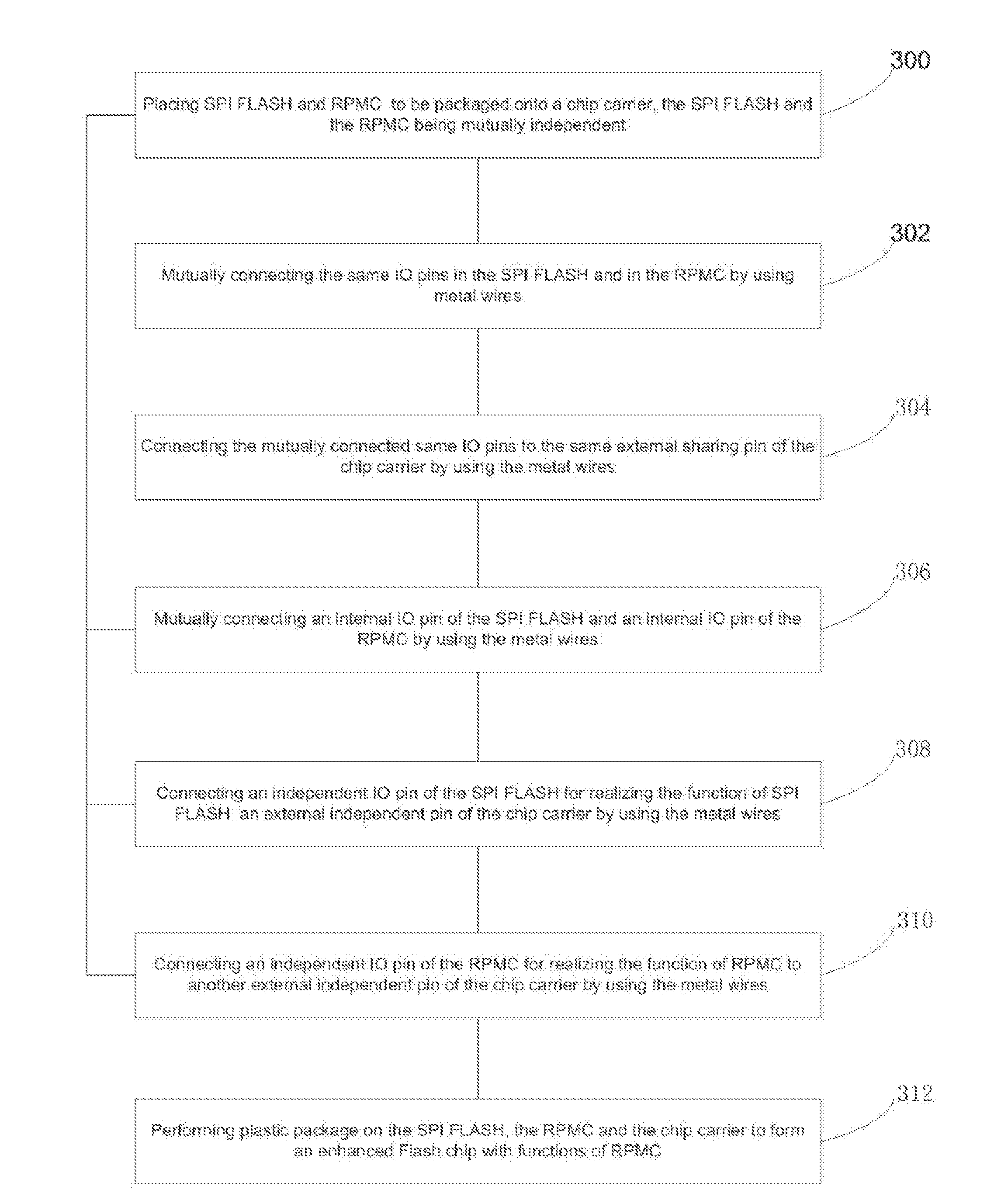
[0044]FIG. 1 shows a schematic diagram of the logical connection of the enhanced Flash chip of SPI interface according to a second embodiment of the present invention.
[0045]As shown in FIG. 1, the enhanced Flash chip of SPI interface according to the embodiment of the present invention may comprise a SPI FLASH and a RPMC which are packaged integrally.
[0046]Herein, the SPI FLASH and the RPMC each comprises a plurality of pins, and the same IO pins in the RPMC and the SPI FLASH may be connected to the same set of external sharing pins. The RPMC and the SPI FLASH may receive an instruction from outside simultaneously response correspondingly. The SPI FLASH and the RPMC may further comprise internal IO pins, respectively, such that the internal IO pins of SPI FLASH and the internal IO pins of RPMC are mutually connected. The RPMC and the SPI F...
third embodiment
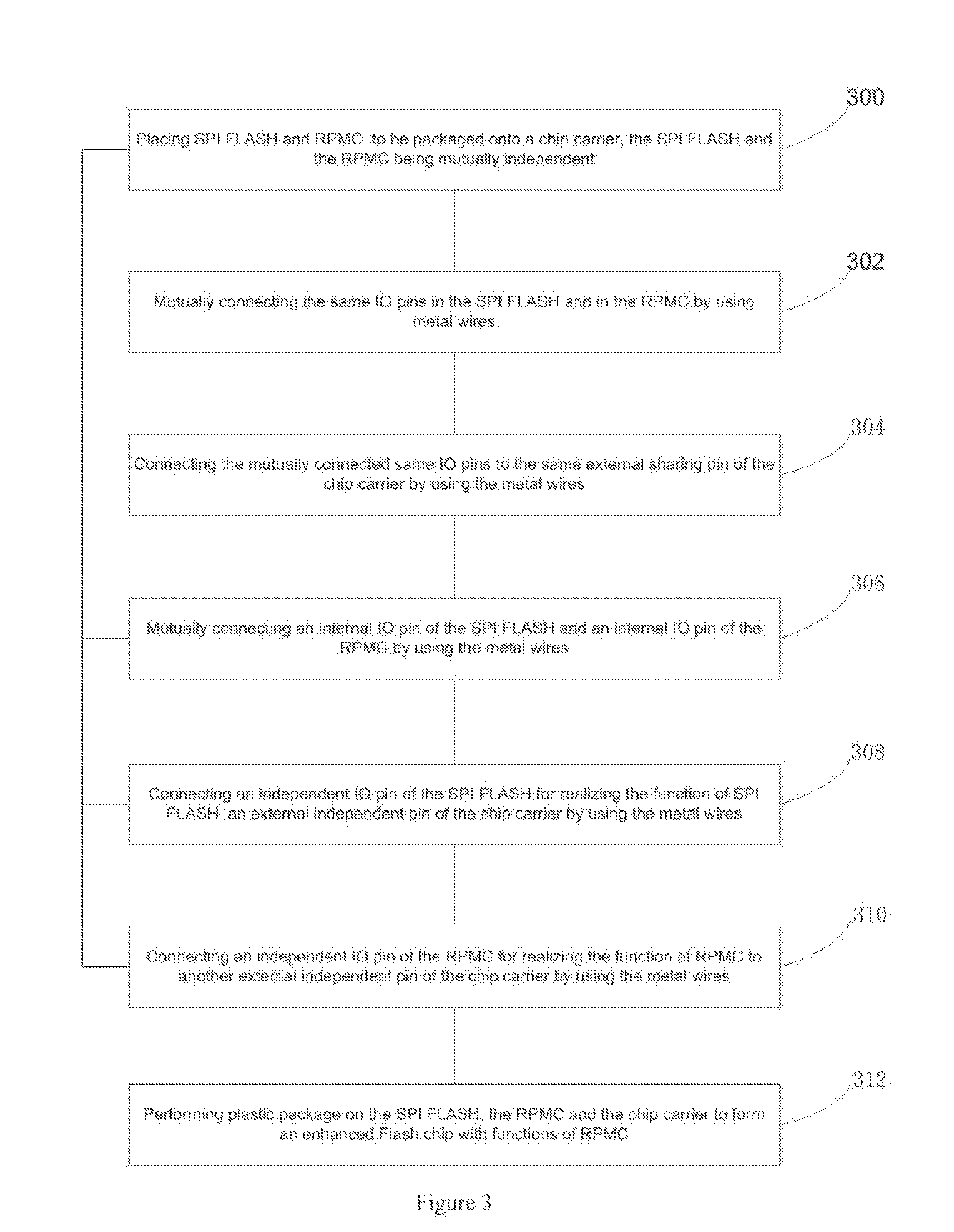
[0110]Hereafter, the specific method for packaging the chip will be explained by way of the third embodiment of the present invention.
[0111]FIG. 3 shows a flow chart of the method for packaging chip according to a third embodiment of the present invention. The packaging method may comprise steps of:
[0112]Step 300: placing SPI FLASH and RPMC to be packaged onto a chip carrier, the SPI FLASH and the RPMC being mutually independent.
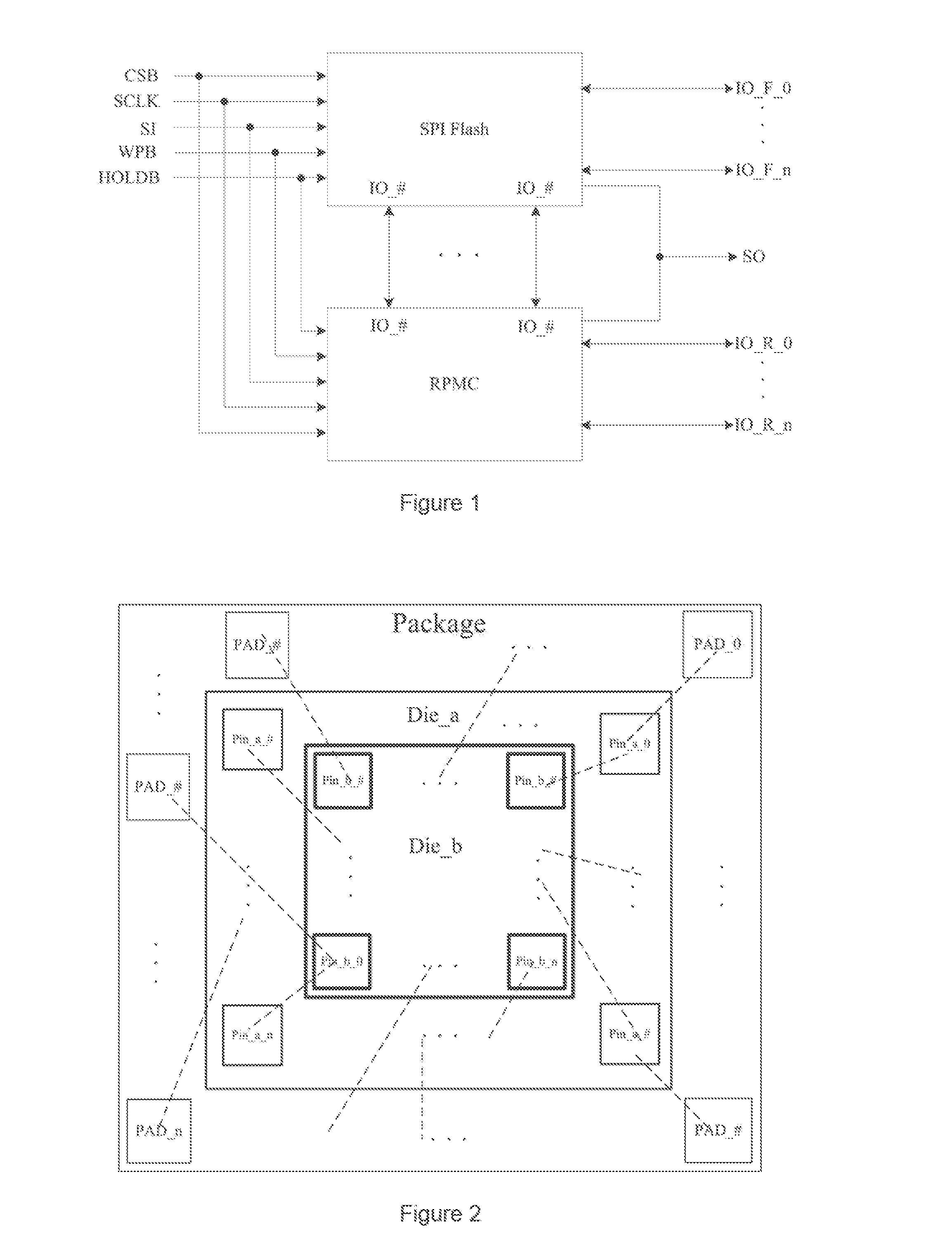
[0113]In this embodiment of the present invention, the SPI FLASH and the RPMC are substantially packaged integrally so as to realize the enhanced Flash chip of SPI interface wherein the SPI FLASH and the RPMC are mutually independent.
[0114]First, the SPI FLASH and the RPMC to be packaged may be placed onto the chip carrier. The chip carrier in this embodiment of the present invention may correspond to Package in FIG. 2.
[0115]Preferably. Step 300 may comprise: placing the SPI FLASH and the RPMC onto the chip carrier side by side, or vertically stacking the SP...
PUM
Abstract
Disclosed are an enhanced Flash chip of SPI interface and a method for packaging chip, to solve the problems of high design complexity, long design period and high design cost. The chip comprises SPI FLASH and RPMC which are packaged integrally; the SPI FLASH and the RPMC comprise an independent controller, respectively; the same IO pins in SPI FLASH and RPMC are mutually connected and are connected to the same external sharing pin of the chip. The SPI FLASH and the RPMC further comprise an internal IO pin, respectively, in which the internal IO pin of SPI FLASH is connected with the internal IO pin of RPMC, and the internal mutual communication between the SPI FLASH and the RPMC is achieved through the mutually connected internal IO pins. Thus, it is possible to reduce the package size, decrease the cost of design, shorten design period and improve performance of the chip.
Description
TECHNICAL FIELD[0001]The present application relates to the field of chip technology, and especially to an enhanced Flash chip of SPI interface and a method for packaging chip.BACKGROUND OF THE INVENTION[0002]The enhanced Flash (one type of memory chip) comprising RPMC (Replay Protection Monotonic Counter) is a featured BIOS (Basic Input-Output System) chip launched by Intel. It comprises a SPI (Serial Peripheral Interface) Flash chip having large capacity and a RPMC circuit. The capacity of SPI FLASH chip can be 8M, 16M, 32M, 64M, 128M, 256M or more in which codes and data of CPU (Central Processing Unit) and BIOS are stored; RPMC circuit may guarantee the security and integrity of reading and writing data. The RPMC circuit and the SPI FLASH integrated therein constitute the hardware platform of the BIOS of PC (Personal Computer) system.[0003]At present, when designing the enhanced Flash chip with RPMC function, a designer usually integrates the SPI Flash having large capacity and ...
Claims
Application Information
Patent Timeline
Application Date:The date an application was filed.
Publication Date:The date a patent or application was officially published.
First Publication Date:The earliest publication date of a patent with the same application number.
Issue Date:Publication date of the patent grant document.
PCT Entry Date:The Entry date of PCT National Phase.
Estimated Expiry Date:The statutory expiry date of a patent right according to the Patent Law, and it is the longest term of protection that the patent right can achieve without the termination of the patent right due to other reasons(Term extension factor has been taken into account ).
Invalid Date:Actual expiry date is based on effective date or publication date of legal transaction data of invalid patent.

