

Optical waveguide and optical device based on the same
a technology of optical waveguides and optical devices, applied in the field of optical devices, can solve the problems of optical waveguides showing a sensitive wavelength characteristic change, optical waveguides with different wavelength characteristics from that of designs, and loss and distortion of signals, so as to achieve fine adjustment of wavelength errors and minimize power consumption. , the effect of easy adjustment of wavelength errors
- Summary
- Abstract
- Description
- Claims
- Application Information
AI Technical Summary
Benefits of technology
Problems solved by technology
Method used
Image

Examples
Embodiment Construction
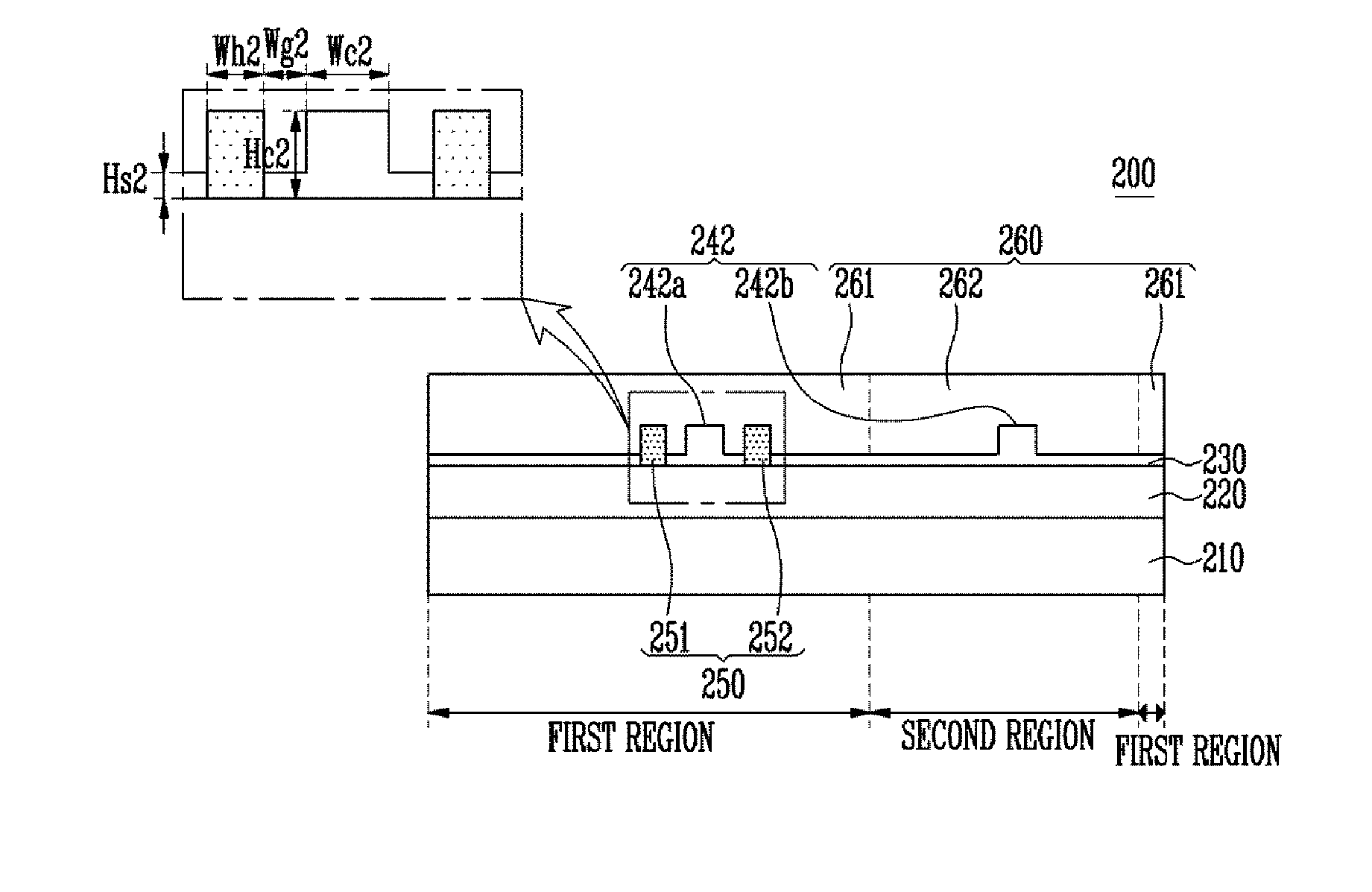
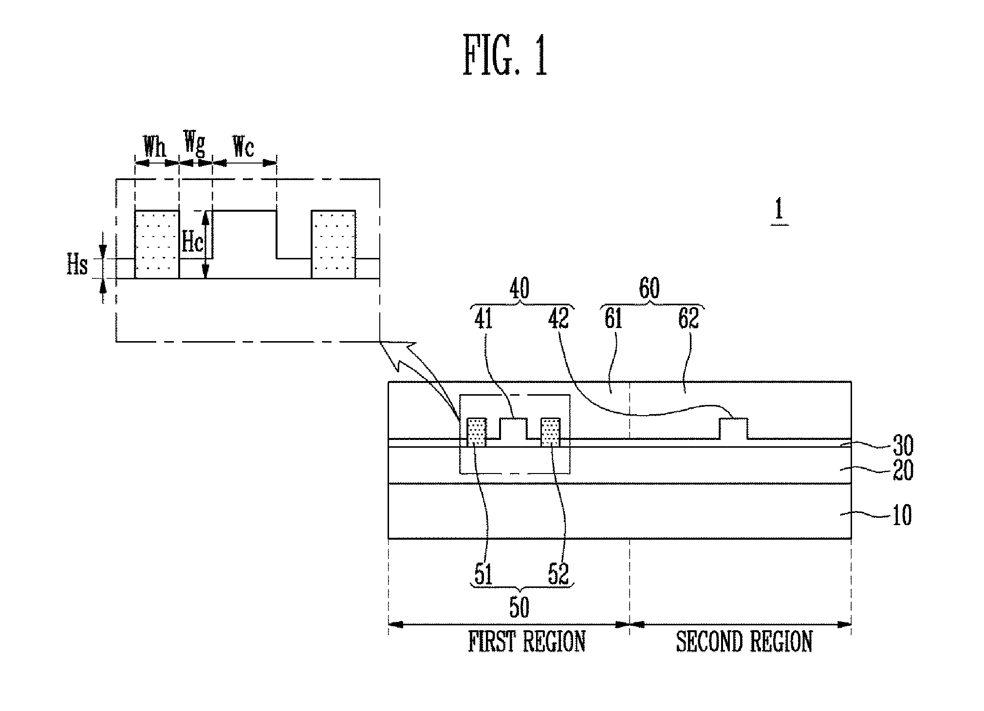
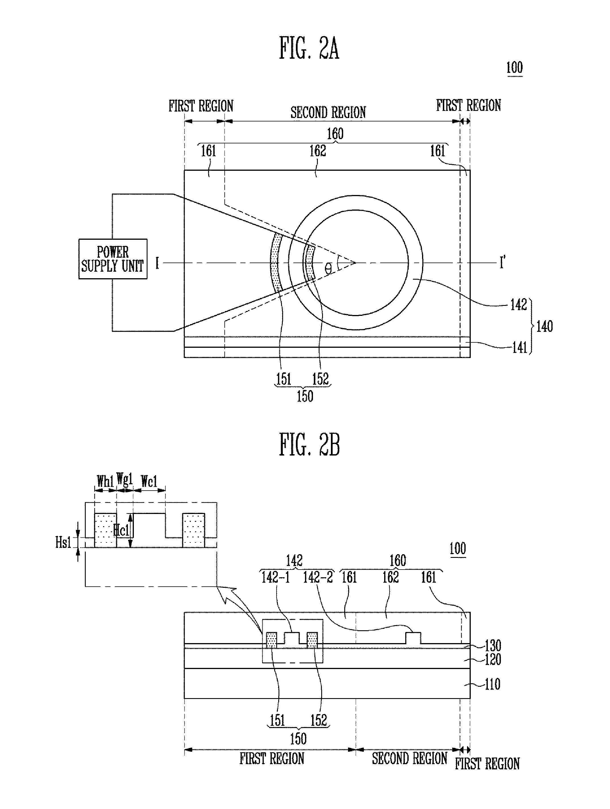
[0041]Hereinafter, the present invention will be described in more detail with reference to drawings to which preferred examples according to the present invention are attached in order to describe the present invention more specifically. As those skilled in the art would realize, the described embodiments may be modified in various different ways, all without departing from the spirit or scope of the present invention.
[0042]It will be understood that when a layer is referred to as being “on” another layer or substrate, it can be directly on the other layer or substrate, or intervening them may also be present. Further, in the present specification, directional expressions, such as an upper side, an upper part, and an upper surface, may be understood as a lower side, a lower part, and a lower surface. That is, the spatial and directional expression should be understood as a relative direction, and should not be limitedly understood as an absolute direction. Also, in the present spec...
PUM
| Property | Measurement | Unit |
|---|---|---|
| wavelength | aaaaa | aaaaa |
| thicknesses | aaaaa | aaaaa |
| widths | aaaaa | aaaaa |
Abstract
Description
Claims
Application Information