Radiographic image detection device

a detection device and radiographic technology, applied in the direction of radiation intensity measurement, instruments, x/gamma/cosmic radiation measurement, etc., can solve the problems of high manufacturing cost, abnormal growth or irregular growth of part of columnar crystals, and increase the manufacturing cost of csi over gos. to achieve the effect of preventing damage to the scintillator

Active Publication Date: 2015-07-23
FUJIFILM CORP
View PDF8 Cites 6 Cited by
  • Summary
  • Abstract
  • Description
  • Claims
  • Application Information

AI Technical Summary

Benefits of technology

[0016]An object of the present invention is to provide an ISS type radiographic image detection device which prevents damage to a scintillator.
[0026]According to the radiographic image detection device of the present invention, the gap layer is provided between the scintillator and the circuit board. Owing to this, the radiographic image detection device prevents damage to the scintillator.

Problems solved by technology

Manufacturing cost using the CsI is more expensive than that using the GOS.
However, the use of the vapor deposition base in the laminated type radiographic image detection device increases manufacturing processes, resulting in high manufacturing cost.
However, the direct vapor deposition type has a drawback that a part of the columnar crystals may grow abnormally or irregularly during the vapor deposition of the scintillator on the photoelectric conversion panel.
Since the end portions of the abnormally-grown crystals expand significantly, the end portions generate a high amount of light, which causes an image defect in a radiographic image.
In a case where the photoelectric conversion panel with the scintillator is accommodated in a housing without crushing the end portions of the abnormally-grown crystals, the end portions, which protrude from the surface of the scintillator, may come into contact with the housing or the like and break when a load is imposed on the housing.
The breakage of the end portions of the abnormally-grown crystals may cause damage to the adjacent normal columnar crystals.
Since a circuit board, on which a signal processor for generating image data and the like are mounted, faces the scintillator in the ISS type, the end portions of the abnormally-grown crystals are likely to come into contact with and be crushed by the circuit board.

Method used


Image

  • Radiographic image detection device
  • Radiographic image detection device
  • Radiographic image detection device

Examples


Embodiment Construction

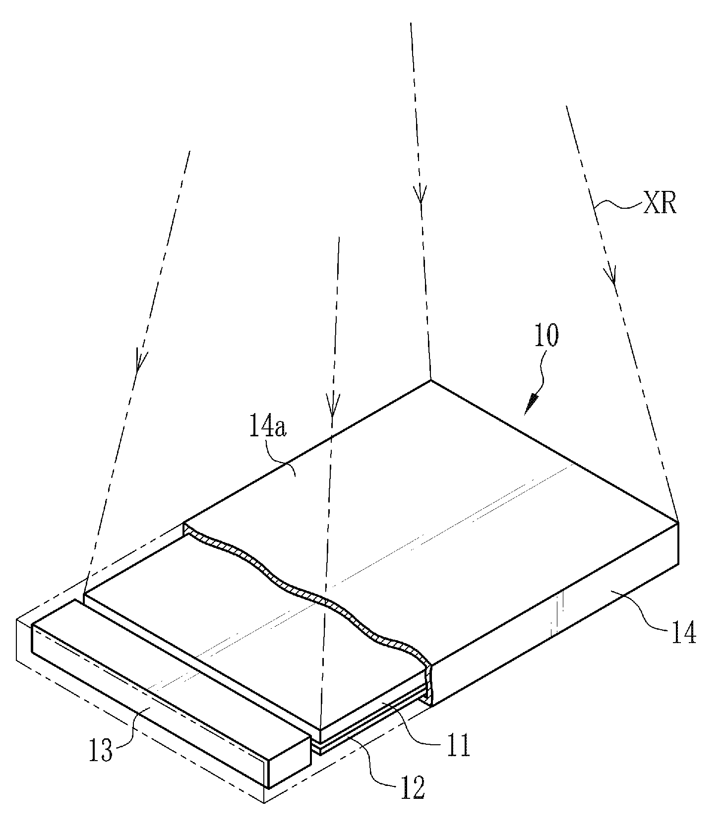
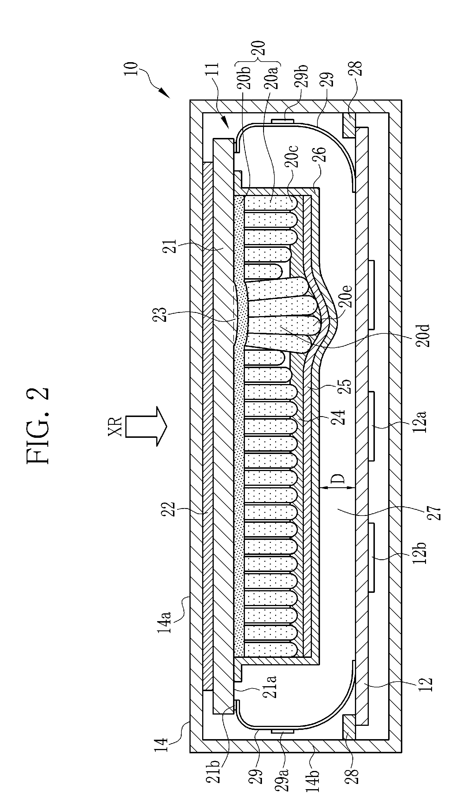
[0040]In FIG. 1, an X-ray image detection device 10 comprises a flat panel detector (FPD) 11, a circuit board 12, a control unit 13, and a housing 14. The housing 14 accommodates the FPD 11, the circuit board 12, and the control unit 13. The housing 14 has an integral monocoque structure made from lightweight carbon fiber reinforced plastics (or carbon fiber) having high X-ray (XR) transmission property and high durability.

[0041]One of the sides of the housing 14 is formed with an opening (not shown). The FPD 11, the circuit board 12, and the control unit 13 are inserted into the housing 14 through the opening at the time of manufacture of the X-ray image detection device 10. A lid (not shown) is attached so as to cover the opening after the insertion.

[0042]At the time of imaging, X-rays XR emitted from an X-ray source 60 (see FIG. 5) and passed through a subject (patient) 61 (see FIG. 5) are applied to a top surface (hereinafter referred to as the exposure surface) 14a of the housi...


PUM


Abstract

A monocoque-structured housing accommodates a photoelectric conversion panel, a scintillator, and a circuit board in this order from an X-ray incidence side. The scintillator contains cesium iodide and converts X-rays into visible light. The scintillator is vapor-deposited on the photoelectric conversion panel. A plurality of pixels that photoelectrically convert the visible light into charges are formed in the photoelectric conversion panel. A signal processor, which reads out the charge from each pixel and generates image data, is mounted on the circuit board. A gap layer is formed between the scintillator and the circuit board.

Description

CROSS-REFERENCE TO RELATED APPLICATIONS[0001]This application is a Continuation of PCT International Application No. PCT / JP2013 / 072661 filed on Aug. 26, 2013, which claims priority under 35 U.S.C. §119(a) to Japanese Patent Application No. 2012-213877, filed Sep. 27, 2012. Each of the above application(s) is hereby expressly incorporated by reference, in its entirety, into the present application.BACKGROUND OF THE INVENTION[0002]1. Field of the invention[0003]The present invention relates to a radiographic image detection device used for radiographic imaging.[0004]2. Description Related to the Prior Art[0005]Recently, radiographic image detection devices have been used for diagnostic imaging in medical fields. The radiographic image detection device converts radiation (for example, X-rays) applied from a radiation source and passed through an object of interest of a subject (patient) into charges and produces a radiographic image. There are direct-conversion type and indirect-conver...

Claims


Application Information

Patent Timeline
Patent Type & Authority Applications(United States)
IPC IPC(8): G01T1/20G01T1/161
CPCG01T1/161G01T1/2018G01T1/202A61B6/4233A61B6/4283G01T1/20189G01T1/20187G01T1/20188
Inventor NARIYUKI, FUMITONABETA, TOSHIYUKIOKADA, YOSHIHIROWATANO, HIROTAKAKATO, MUNETAKANAKATSUGAWA, HARUYASU
Owner FUJIFILM CORP
Why Eureka
Try Eureka