Semiconductor Device

a technology of semiconductor devices and components, applied in the field of semiconductor devices, can solve the problem of high component densities and other problems

Active Publication Date: 2015-07-23
MICRO MODULE TECH
View PDF0 Cites 9 Cited by
  • Summary
  • Abstract
  • Description
  • Claims
  • Application Information

AI Technical Summary

Benefits of technology

[0010]The present invention can realize further miniaturization of a semiconductor device having a switching element and a diode.

Problems solved by technology

However, higher component densities are required due to miniaturization and multifunction of products in recent years.

Method used


Image

  • Semiconductor Device
  • Semiconductor Device
  • Semiconductor Device

Examples


Embodiment Construction

[0029]Embodiments of the present invention will be described hereinafter with reference to drawings.

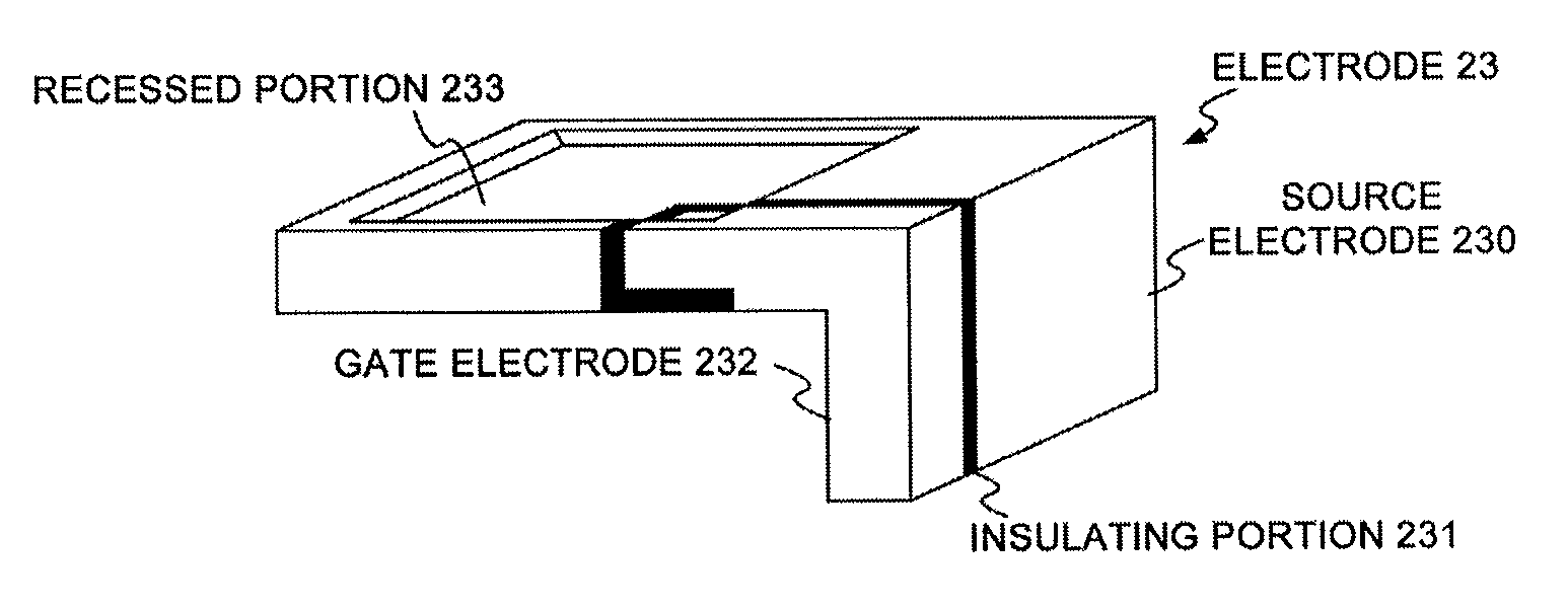
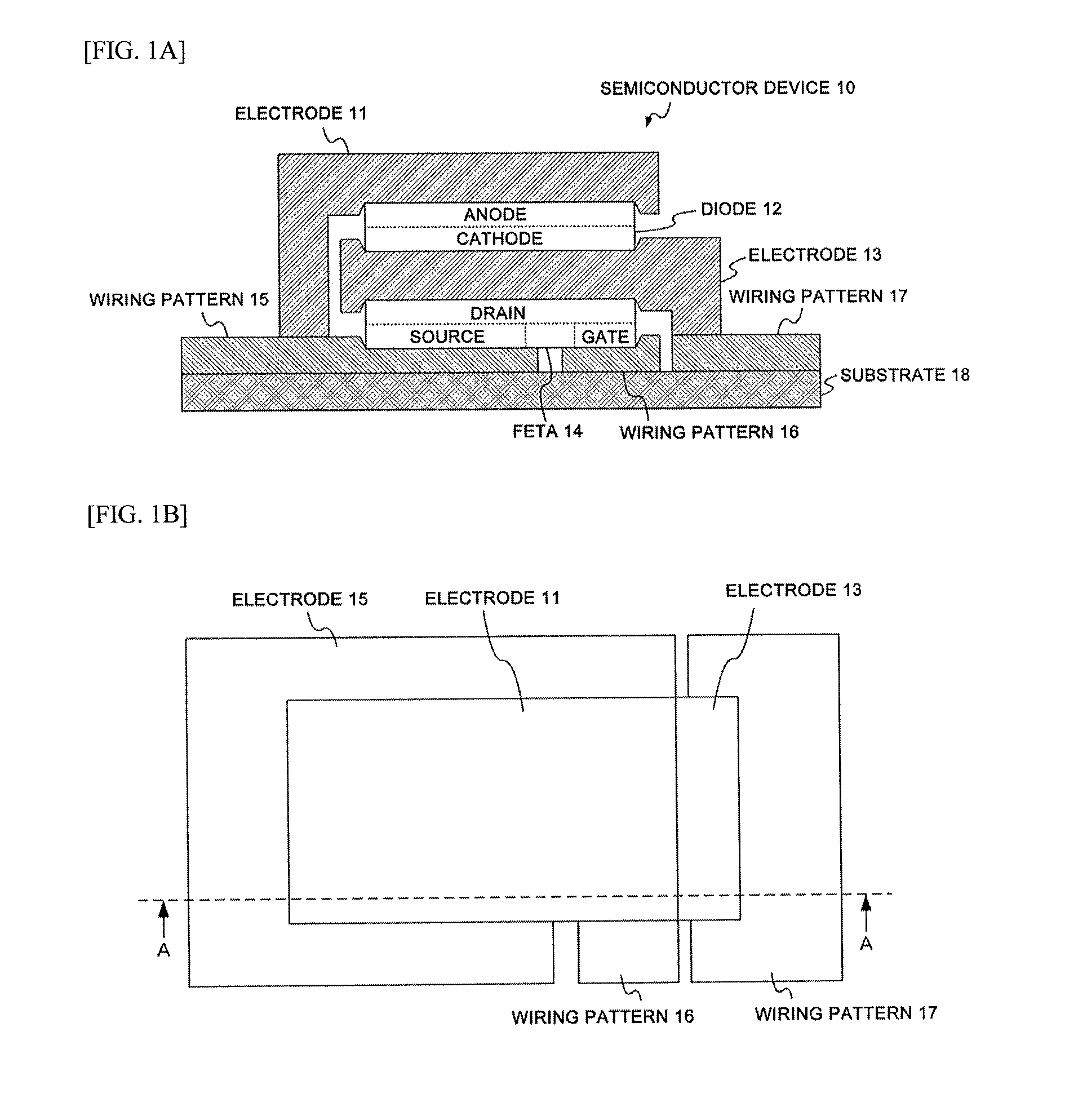
[0030]FIG. 1A is a cross-sectional view and FIG. 1B is a plan view illustrating one example of a structure of a semiconductor device 10 according to one embodiment of the present invention. FIG. 1A is a cross-sectional diagram along the line A-A of the semiconductor device 20 of FIG. 1B. The semiconductor device 10 is provided with an electrode 11, a diode 12, an electrode 13, a field effect transistor (FET) 14, a wiring pattern 15, a wiring pattern 16, a wiring pattern 17, and a substrate 18. The FET 14 is one example of a switching element.

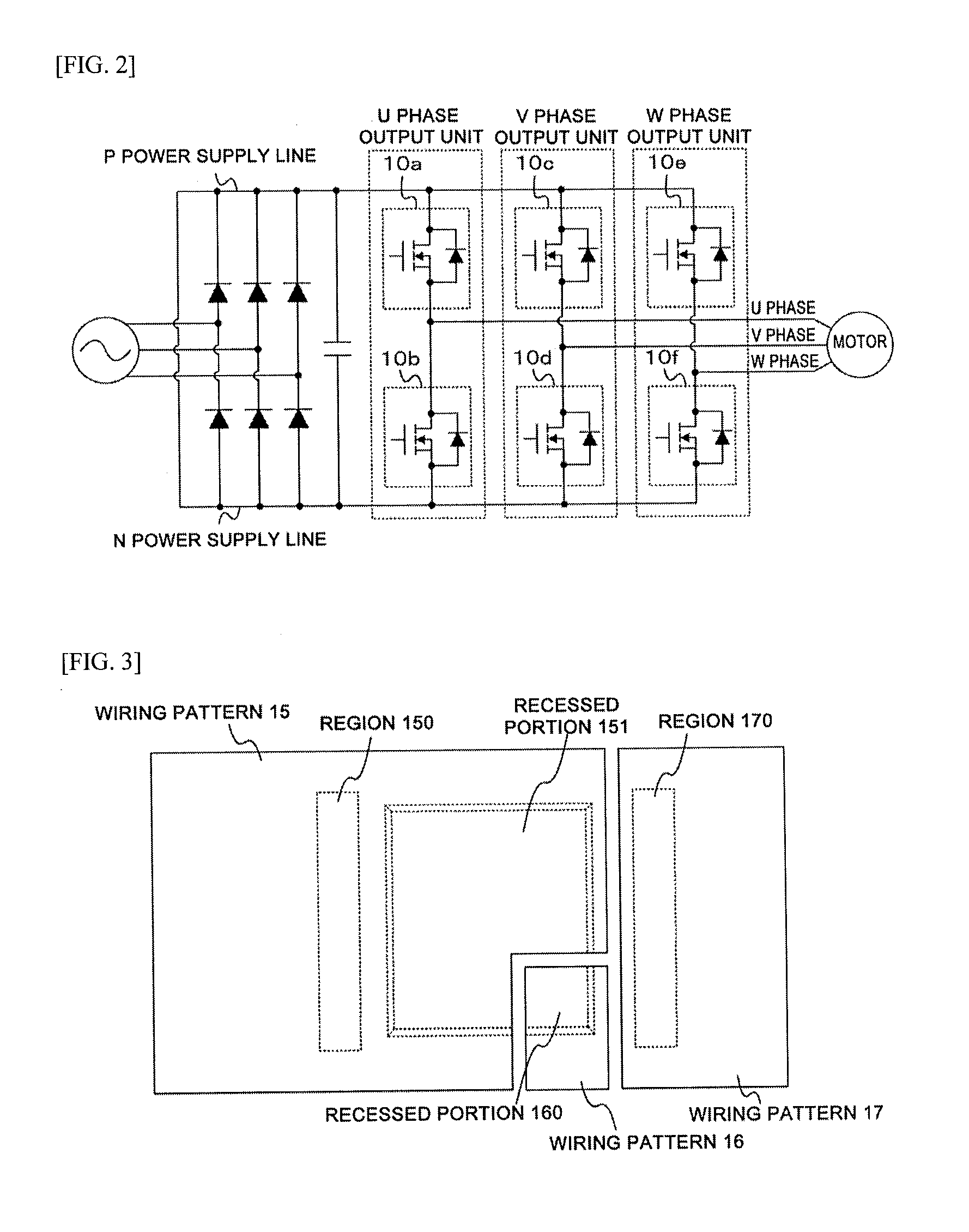
[0031]The semiconductor device 10 illustrated in this embodiment can be used in a circuit such as that illustrated for example in FIG. 2. The circuit illustrated in FIG. 2, is a power converter circuit configured of a three-phase pulse width modulation (PWM) inverter, and has a U phase output unit, V phase output unit, and W phase output unit prov...


PUM


Abstract

To realize further miniaturization of a semiconductor device.
The semiconductor device 10 is provided with a switching element (FET 14) provided on a substrate 18, a first electrode (electrode 13) provided on an opposite side of the substrate 18 interposing the switching element, a diode 12 provided on an opposite side of the switching element interposing the first electrode, and a second electrode (electrode 11) provided on an opposite side of the first electrode interposing the diode 12.

Description

FIELD OF THE INVENTION[0001]The present invention relates to a semiconductor device. The present invention claims priority from Japanese Patent Application Number 2012-205618 filed on Sep. 19, 2012, and the content of that application is hereby incorporated by reference into the present application, for designated countries that recognize incorporation of documents by reference.BACKGROUND OF THE INVENTION[0002]A power module where a switching element, such as a MOSFET or the like, and a flywheel diode are disposed side by side on a single substrate is disclosed in Patent Document 1 below.PRIOR ART DOCUMENTSPatent Documents[0003]Patent Document 1: Japanese Unexamined Patent Application Publication No. 2009-105389ASUMMARY OF THE INVENTIONDescription of the Related Art[0004]However, higher component densities are required due to miniaturization and multifunction of products in recent years. Further miniaturization is also required for the power module described in Patent Document 1 abo...

Claims


Application Information

Patent Timeline
Patent Type & Authority Applications(United States)
IPC IPC(8): H01L25/18H01L23/367H01L29/861H01L29/78H01L29/739H01L23/528H01L23/31
CPCH01L25/18H01L23/528H01L23/3675H01L29/861H01L29/7827H01L29/7802H01L29/7395H01L23/3107H01L24/29H01L24/32H01L24/83H01L2224/26175H01L2224/291H01L2224/29339H01L2224/8314H01L2224/83385H01L2924/15153H01L2224/29294H01L2924/13091H01L23/4334H01L23/49575H01L23/49838H01L2224/32245H01L2224/33181H01L2924/13055H01L2924/1305H01L23/49524H01L23/49534H01L23/49562H01L23/49816H01L23/49844H01L23/3128H01L24/40H01L24/41H01L2224/83801H01L2224/8384H01L2224/37147H01L2224/40095H01L24/37H01L2924/00014H01L25/074H01L2224/0603H01L2924/014H01L2924/00H01L2224/84
Inventor HARAZONO, FUMIKAZU
Owner MICRO MODULE TECH
Why Eureka
Try Eureka