Parallelogram cell design for high speed vertical channel 3D NAND memory

a parallelogram cell, 3d nand technology, applied in the direction of basic electric elements, semiconductor devices, electrical equipment, etc., can solve the problems of increasing the number of memory layers, increasing power consumption and slowing device operation, and introducing significant process challenges, so as to increase the data rate, increase the parallel operation, and the density of bit lines

Active Publication Date: 2015-07-23
MACRONIX INT CO LTD
View PDF2 Cites 51 Cited by
  • Summary
  • Abstract
  • Description
  • Claims
  • Application Information

AI Technical Summary

Benefits of technology

[0014]Roughly described, the present technology provides a memory device having a multilevel stack of conductive layers oriented parallel to a substrate. Pillars oriented orthogonally to the substrate each include series-connected memory cells at cross-points between the pillars and the conductive layers. String select lines (SSLs) are disposed above the conductive layers, each intersection of a pillar and an SSL defining a respective select gate of the pillar. Bit lines are disposed above the string select lines. The pillars in the plurality of pillars are arranged on a regular grid having a unit cell which is a non-rectangular parallelogram. The pillars may be arranged so as to define a number of parallel pillar lines, the pillar lines having an acute angle 0>0° of intersection with the bit line conductors, each line of pillars having exactly n>1 pillars all intersecting a particular common one of the string select lines. The arrangement permits a higher density of bit lines, thereby enabling a higher data rate due to increased parallel operation. It also enables a smaller number of SSLs, thereby reducing disturbance, reducing power consumption and further improving data rate by reducing unit cell capacitance.

Problems solved by technology

While 3D stacking memory structures hold the promise of greatly increased memory density, they also introduce significant process challenges because, among other things, of the need to etch very deep holes through many layers.
Unit cell capacitance also increases with the number of SSLs 12, thereby increasing power consumption and slowing device operation.
Thus increasing the number of memory layers also increases the number of SSLs 12, and again increases power consumption and slows device operation.

Method used


Image

  • Parallelogram cell design for high speed vertical channel 3D NAND memory
  • Parallelogram cell design for high speed vertical channel 3D NAND memory
  • Parallelogram cell design for high speed vertical channel 3D NAND memory

Examples


Embodiment Construction

[0024]The following description is presented to enable any person skilled in the art to make and use the invention, and is provided in the context of a particular application and its requirements. Various modifications to the disclosed embodiments will be readily apparent to those skilled in the art, and the general principles defined herein may be applied to other embodiments and applications without departing from the spirit and scope of the present invention. Thus, the present invention is not intended to be limited to the embodiments shown, but is to be accorded the widest scope consistent with the principles and features disclosed herein.

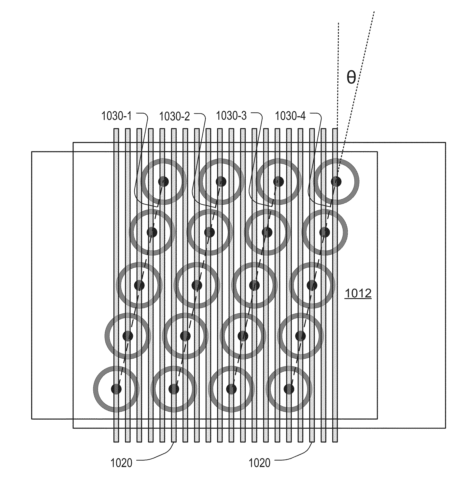
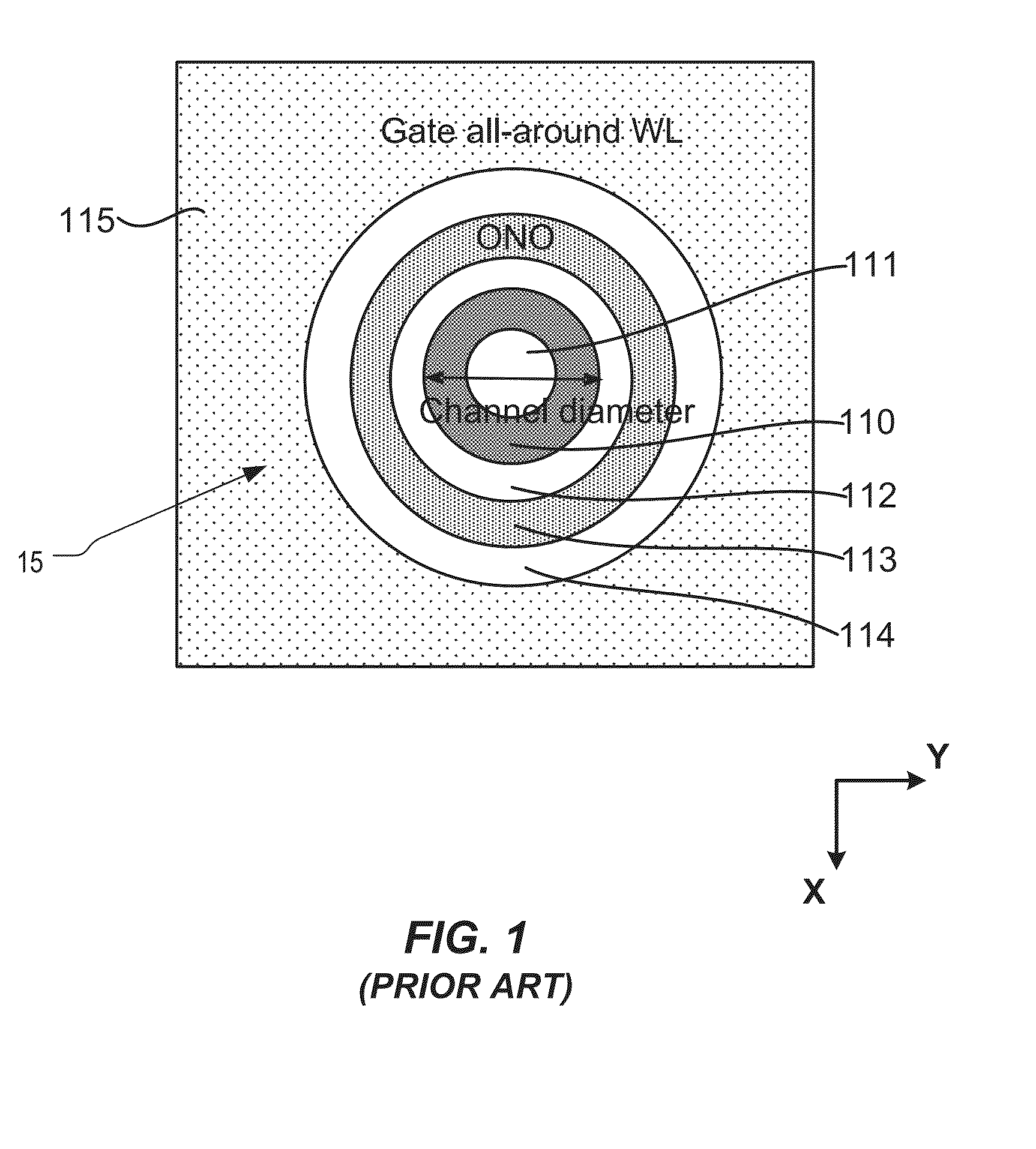
[0025]FIG. 5 is a top view of an example array of pillars in a conventional 3D structure such as that shown in FIGS. 2 and 4. Each dot in FIG. 5 represents the lateral position of a corresponding pillar 515. As used herein, “lateral” dimensions refer to dimensions of the structure which are parallel to the substrate (e.g. dimensions labeled X a...


PUM


Abstract

Roughly described, a memory device has a multilevel stack of conductive layers. Pillars oriented orthogonally to the substrate each include series-connected memory cells at cross-points between the pillars and the conductive layers. String select lines (SSLs) are disposed above the conductive layers, and bit lines are disposed above the SSLs. The pillars are arranged on a regular grid having a unit cell which is a non-rectangular parallelogram. The pillars may be arranged so as to define a number of parallel pillar lines, each having an acute angle θ>° relative to the bit line conductors, each line of pillars having n>1 pillars intersecting a common one of the SSL. The arrangement permits higher bit line density, a higher data rate due to increased parallelism, and a smaller number of SSLs, thereby reducing disturbance, reducing power consumption and reducing unit cell capacitance.

Description

CROSS-REFERENCE TO OTHER APPLICATIONS[0001]This application is a Continuation-In-Part of U.S. application Ser. No. 14 / 157,550, filed 17 Jan. 2014, entitled THREE-DIMENSIONAL SEMICONDUCTOR DEVICE (P1020208), incorporated by reference herein.[0002]This application also makes reference to U.S. application Ser. No. ______, filed on even date herewith, entitled TWISTED ARRAY DESIGN FOR HIGH SPEED VERTICAL CHANNEL 3D NAND MEMORY, by inventor Shih-Hung Chen (P1030081US, Docket No. MXIC 2132-1), incorporated by reference herein.BACKGROUND[0003]1. Field of the Invention[0004]The present invention relates to high density memory devices, and particularly to memory devices in which multiple planes of memory cells are arranged to provide a three-dimensional 3D array.[0005]2. Description of Related Art[0006]As critical dimensions of devices in integrated circuits shrink to the limits of common memory cell technologies, designers have been looking to techniques for stacking multiple planes of memo...

Claims


Application Information

Patent Timeline
Patent Type & Authority Applications(United States)
IPC IPC(8): H01L27/115H01L29/423
CPCH01L27/11582H01L29/42344H01L27/11565H01L27/0207H10B43/35H10B43/10H10B43/27H10B43/20
Inventor CHEN, SHIH-HUNG
Owner MACRONIX INT CO LTD
Why Eureka
Try Eureka