MEMS package structure

a technology of microelectromechanical systems and package structures, applied in the direction of optical elements, instruments, and details of semiconductor/solid-state devices, can solve the problem of extreme fragility of the semiconductor device, and achieve the effect of reducing the height of the peripheral gap and improving the moisture resistance property

Active Publication Date: 2015-07-30
HIMAX DISPLAY INC
View PDF1 Cites 6 Cited by
  • Summary
  • Abstract
  • Description
  • Claims
  • Application Information

AI Technical Summary

Benefits of technology

[0019]Based on the above-mentioned description, the MEMS package structure of the present invention applies the lid having the recess for accommodating the MEMS device so as to reduce the height of the peripheral gap between the chip and the lid, the sealant disposed between the peripheral gap seals the recess, so that the MEMS package structure of the present invention provides better moisture resistance property. In addition, the first moisture barrier coated around the chip, the lid and the sealant provides a double protection to prevent the moisture from permeating to the recess. Besides, the second moisture barrier provides a third protection to seal the chip, the MEMS device, the lid, the sealant and the first moisture barrier in the cavity enclosed by the first substrate and the second substrate. Moreover, the molding compound disposed in the cavity is glued around the first moisture barrier to provide a fourth protection. Furthermore, the moisture absorption element disposed in the cavity provides a fifth protection to absorb the moisture in the cavity.

Problems solved by technology

However, in the macroscopic world of the entire package structure, the MEMS device is extremely fragile and may be impacted by slight static electricity or surface tension at any moment to cause failure.

Method used


Image

  • MEMS package structure
  • MEMS package structure
  • MEMS package structure

Examples


Embodiment Construction

[0025]Reference will now be made in detail to the present preferred embodiments of the invention, examples of which are illustrated in the accompanying drawings. Wherever possible, the same reference numbers are used in the drawings and the description to refer to the same or like parts.

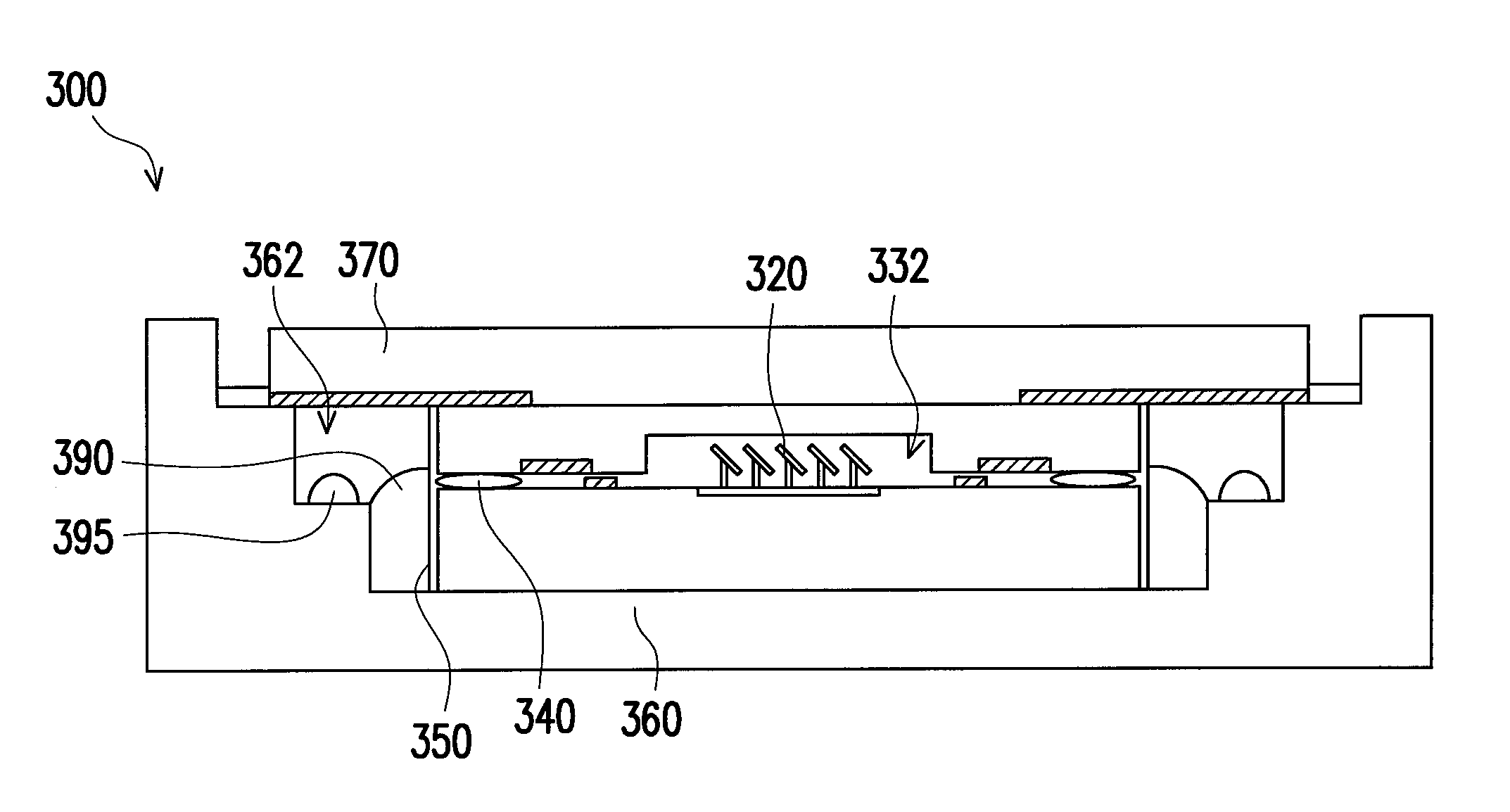
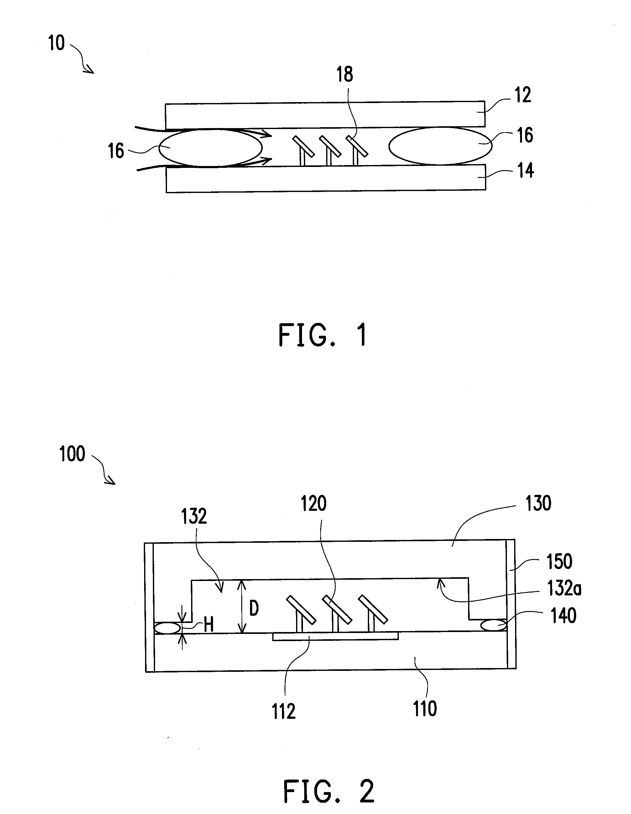
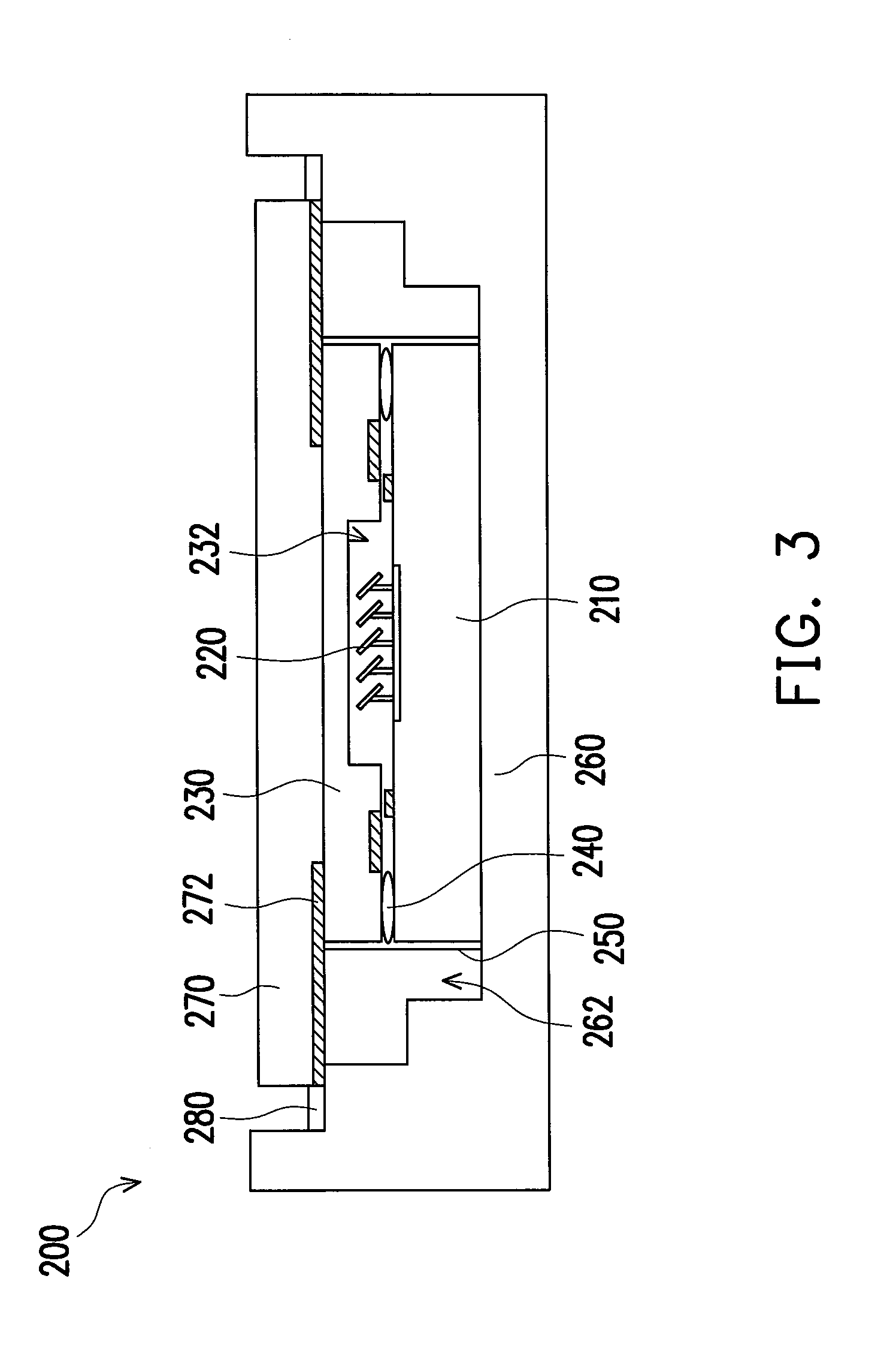
[0026]FIG. 2 is a schematic view of a MEMS package structure according to an embodiment of the invention. Referring to FIG. 2, a microelectromechanical system (MEMS) package structure 100 of the embodiment comprises a chip 110, at least one MEMS device 120, a lid 130, a sealant 140 and a first moisture barrier 150. The chip 110 comprises an active surface 112. The chip 110 is, for example, an optical sensor chip such as a charge couple device (CCD) or a complementary metal-oxide-semiconductor (CMOS), and the active surface 112 is, for example, a photo sensitive region. But the types of the chip 110 and the active surface 112 are not limited thereto.

[0027]The MEMS devices 120 are disposed on the activ...


PUM


Abstract

A MEMS package structure including a chip, a MEMS device, a lid, a sealant and a first moisture barrier is provided. The chip comprises an active surface. The MEMS system device is disposed on the active surface. The lid is covered on the chip and comprising a recess, wherein the MEMS device is in the recess. The sealant is disposed between the chip and the lid so as to seal the recess, wherein a thickness of the sealant is less than a height of the MEMS device. The first moisture barrier is sealed around the chip, the sealant and the lid.

Description

BACKGROUND OF THE INVENTION[0001]1. Field of the Invention[0002]The present invention generally relates to a chip package structure. More particularly, the present invention relates to a microelectromechanical system (MEMS) package structure.[0003]2. Description of Related Art[0004]Microelectromechanical system (MEMS) is a microelectromechanical device fabricated in a microminiaturized package structure, and the fabricating technique thereof is quite similar to the technique of fabricating integrated circuits (ICs). However, interactions, for example, about mechanics, optics, or magnetic force between the MEMS device and surrounding environment are more than that of the conventional IC.[0005]The MEMS device may include micro-sized electromechanical components (for example, switches, mirrors, capacitors, accelerometers, sensors, capacitive sensors, or actuators etc.), and the MEMS device may be integrated with the IC in a manner of single block, thereby greatly modifying insertion lo...

Claims


Application Information

Patent Timeline
Patent Type & Authority Applications(United States)
IPC IPC(8): B81B7/00G02B27/00G02B5/08
CPCG02B27/0006B81B7/0041G02B26/0833B81C2203/019B81C1/00269H01L2924/16235
Inventor SU, CHUN-HAOGELDER, ROLAND V.NAUTA, TORECHEN, WEI-HSIAO
Owner HIMAX DISPLAY INC
Why Eureka
Try Eureka