
Eureka
For R&D, Eureka makes reading and utilizing patents & technical documents easy.
Eureka AIR
Designed for self-driven R&D workflows. Generate viable solutions, solve complex R&D challenges, empower your innovation with AI.

Eureka Materials
Designed for material experts only. Revolutionize your material R&D, from search, analyze, to developing new materials.

TechResearch
Generate reliable direction feasibility study reports for your R&D in just a few steps.

TechSeek
Discover and master advanced knowledge NOW. Basics, ideas, possibilities, all at once.

TechMind
As an expert in R&D Theories, TechMind can generates customized viable solutions instantly.

TechRisk
Analyze your overall solution with one click, know your potential R&D risks in advance.

TechMonitor
Get weekly tech updates, stay abreast of the latest tech innovations and key insights.
Memory Interface
- Summary
- Abstract
- Description
- Claims
- Application Information
AI Technical Summary
Benefits of technology
Problems solved by technology
Method used
Image

Examples
Embodiment Construction
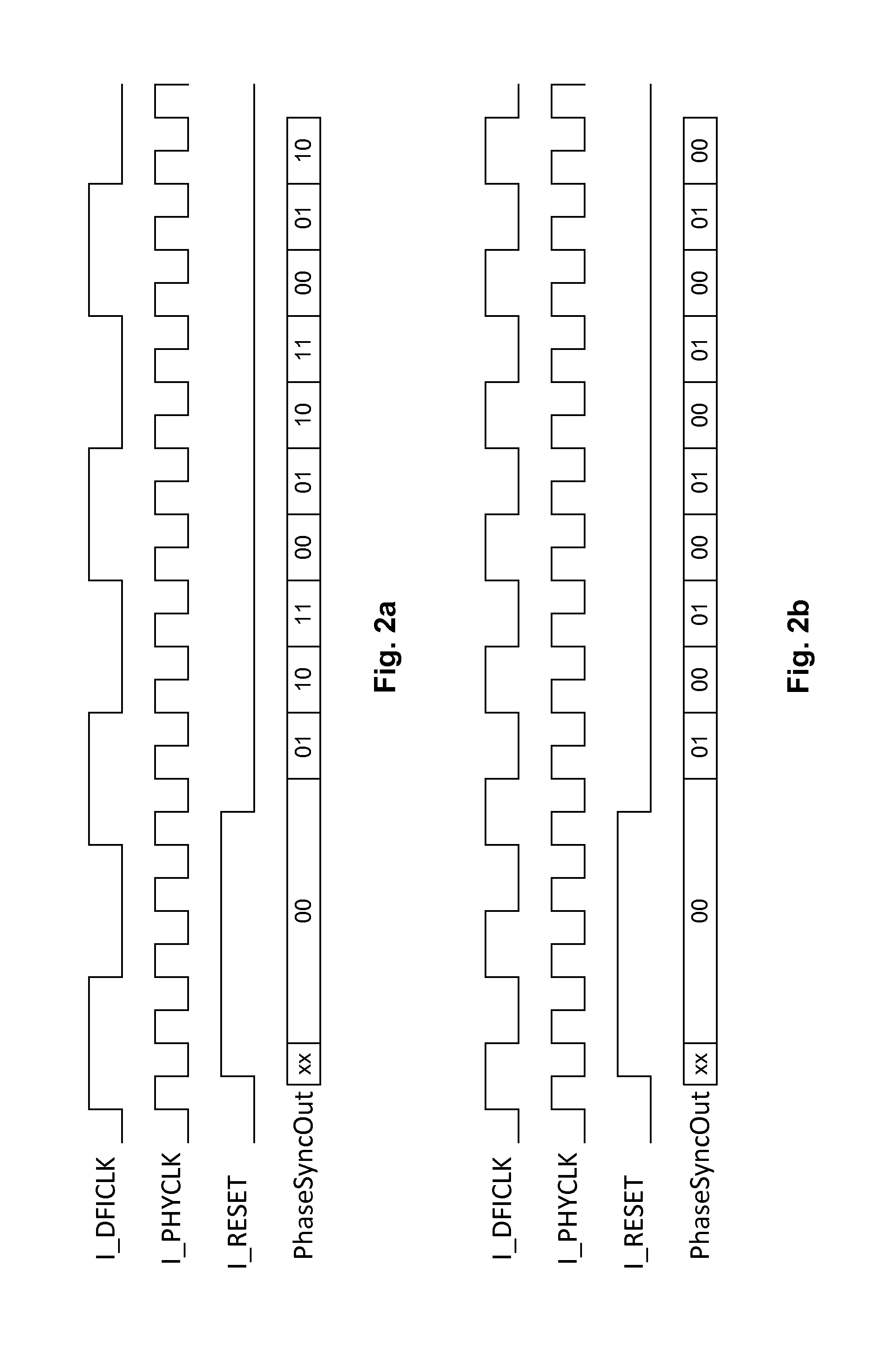
[0020]In the following detailed description of the embodiments, reference is made to the accompanying drawings, which form a part hereof, and in which is shown by way of illustration of specific embodiments in which the present invention may be practiced. The present invention is disclosed in reference to a data path interface between a physical layer interface (“DFI”) of a computing device and a memory device (e.g., an off-chip dynamic random-access memory (“DRAM”)), where the DFI and the DRAM operate in different clock domains. However, it is understood by a person having ordinary skill in the art that the present invention can be applicable to interfacing other modules that operate in different clock domains.
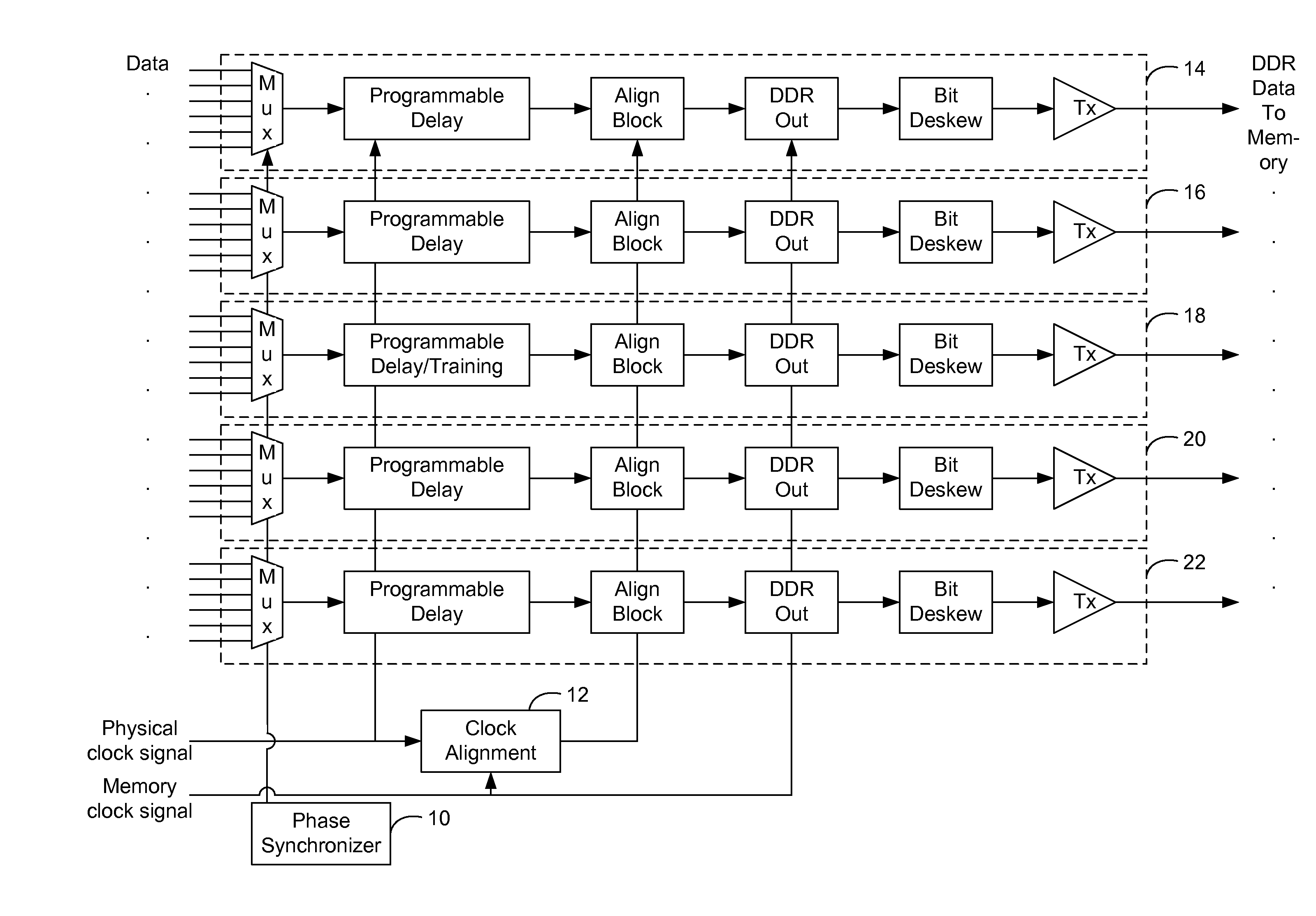
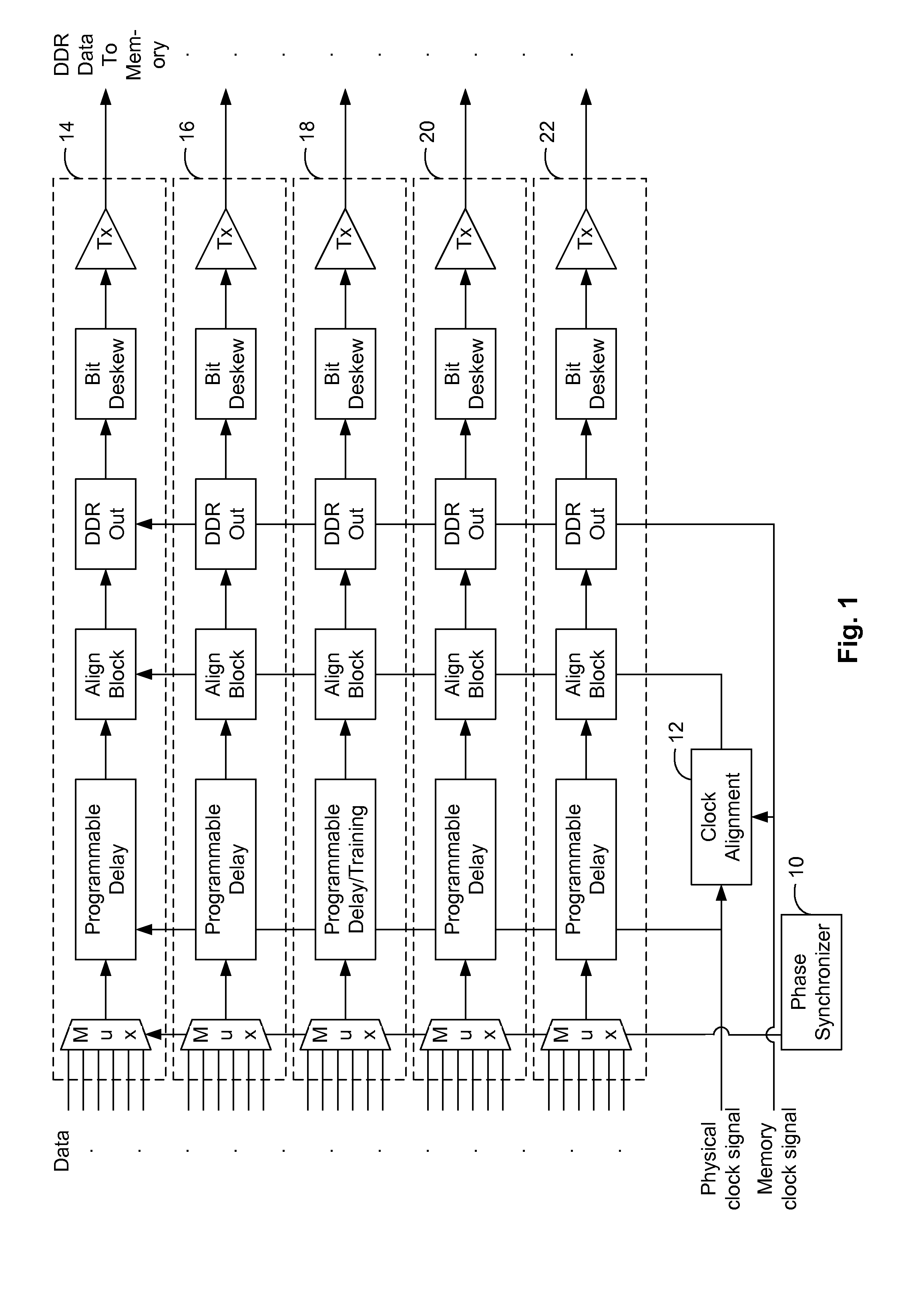
[0021]FIG. 1 illustrates a block diagram of a data path interface of the present invention between a DFI and DRAM. A data path interface of the present invention can provide a data write path between a double data rate (“DDR”) physical layer interface and a DRAM. The DFI prot...
PUM
 Abstract
Description
Claims
Application Information
 - R&D Engineer
- R&D Manager
- IP Professional
- Industry Leading Data Capabilities
- Powerful AI technology
- Patent DNA Extraction
Browse by: Latest US Patents, China's latest patents, Technical Efficacy Thesaurus, Application Domain, Technology Topic, Popular Technical Reports.
© 2024 PatSnap. All rights reserved.Legal|Privacy policy|Modern Slavery Act Transparency Statement|Sitemap|About US| Contact US: help@patsnap.com