Pattern Inspecting and Measuring Device and Program

a technology of measuring device and pattern, applied in image data processing, instruments, image enhancement, etc., to achieve the effect of increasing the reliability of inspection or measurement results and reducing the influence of noise and the lik

Active Publication Date: 2015-08-13
HITACHI HIGH-TECH CORP
View PDF2 Cites 57 Cited by
  • Summary
  • Abstract
  • Description
  • Claims
  • Application Information

AI Technical Summary

Benefits of technology

[0016]According to the present invention, during inspection or measurement using the position of the edge extracted from the image data obtained by imaging the pattern ...

Problems solved by technology

Further, as the shape of the pattern transferred on the wafer becomes more complex, the uses are increasing, for both the inspecting device and th...

Method used


Image

  • Pattern Inspecting and Measuring Device and Program
  • Pattern Inspecting and Measuring Device and Program
  • Pattern Inspecting and Measuring Device and Program

Examples


first example

First Embodiment

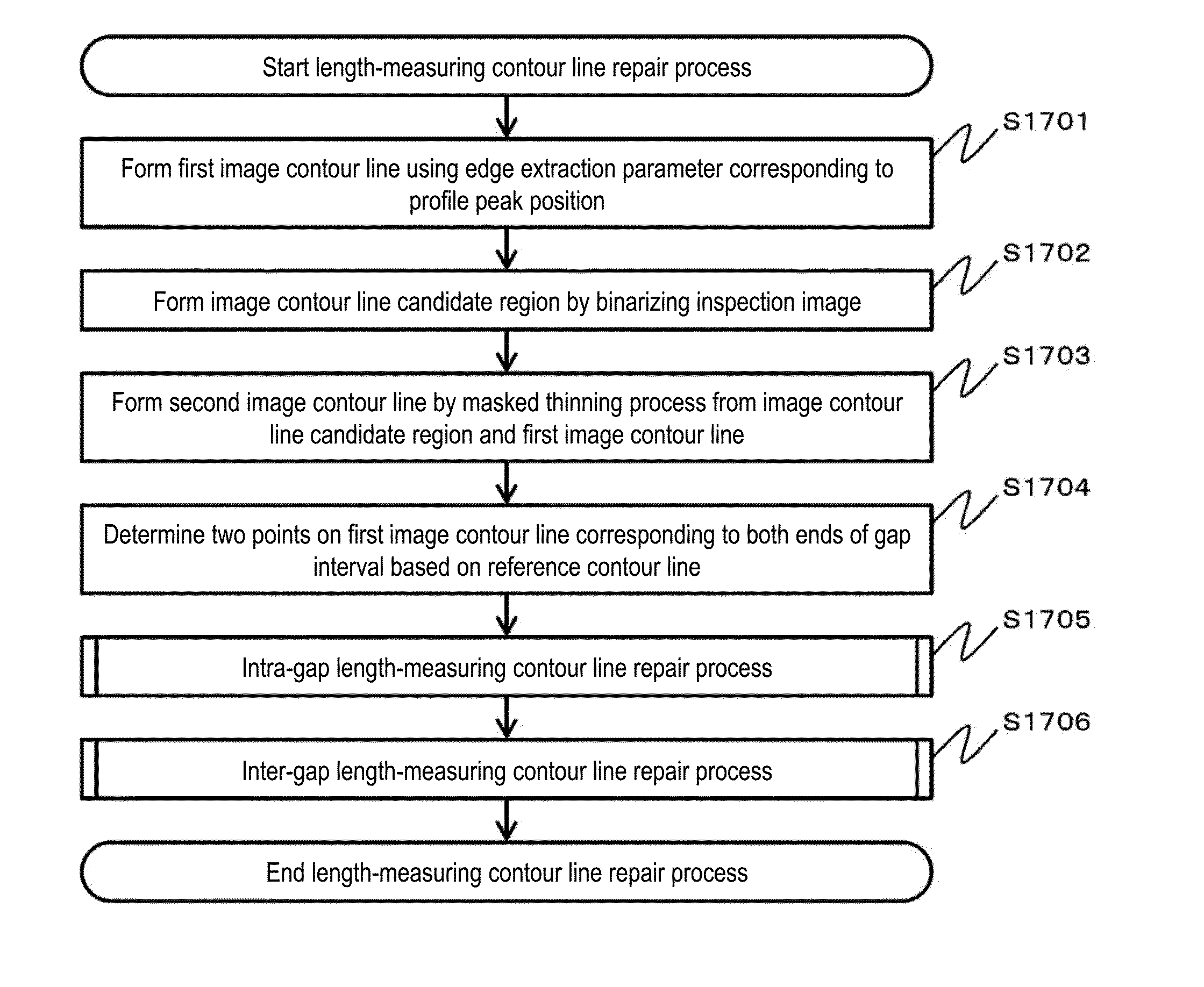
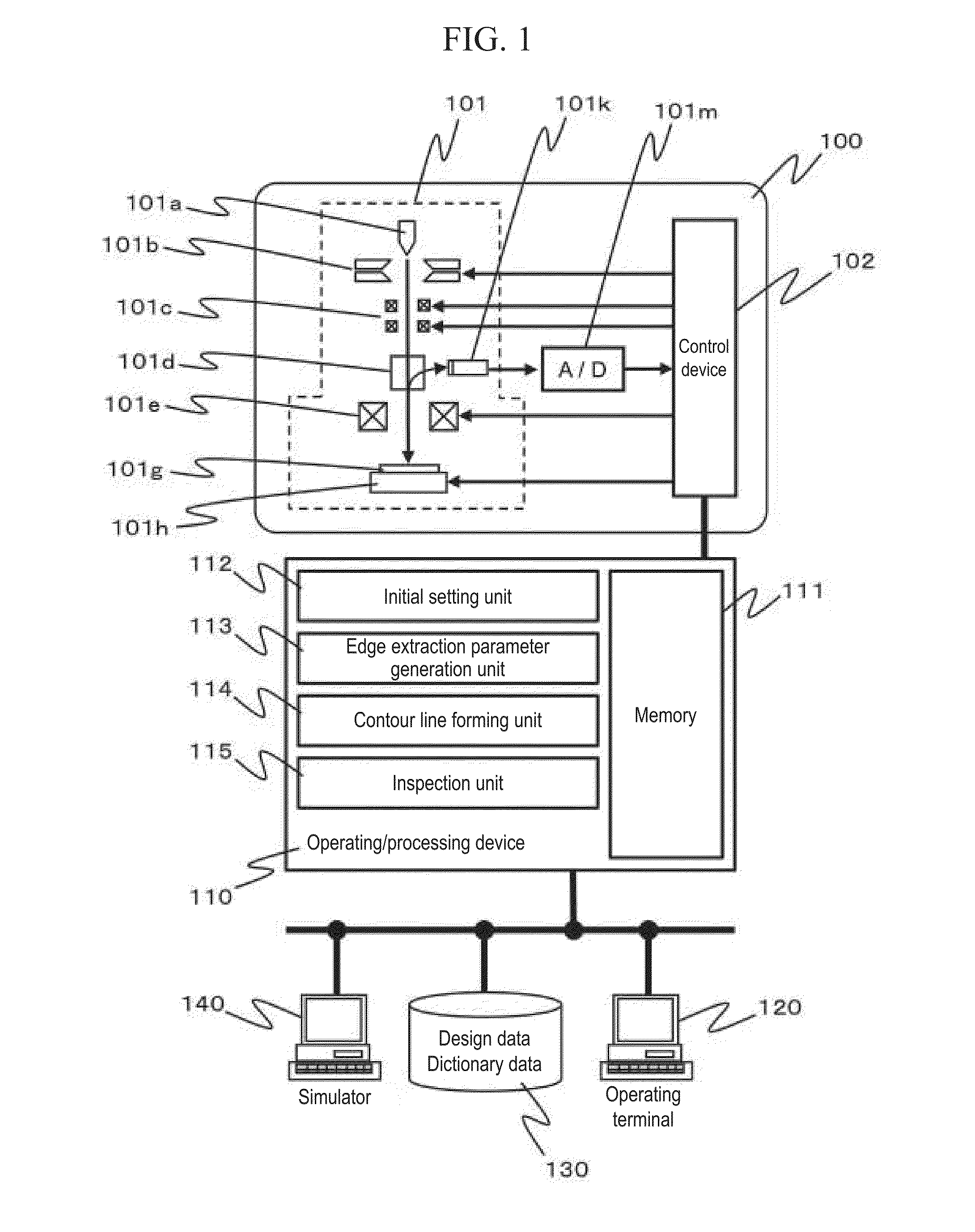
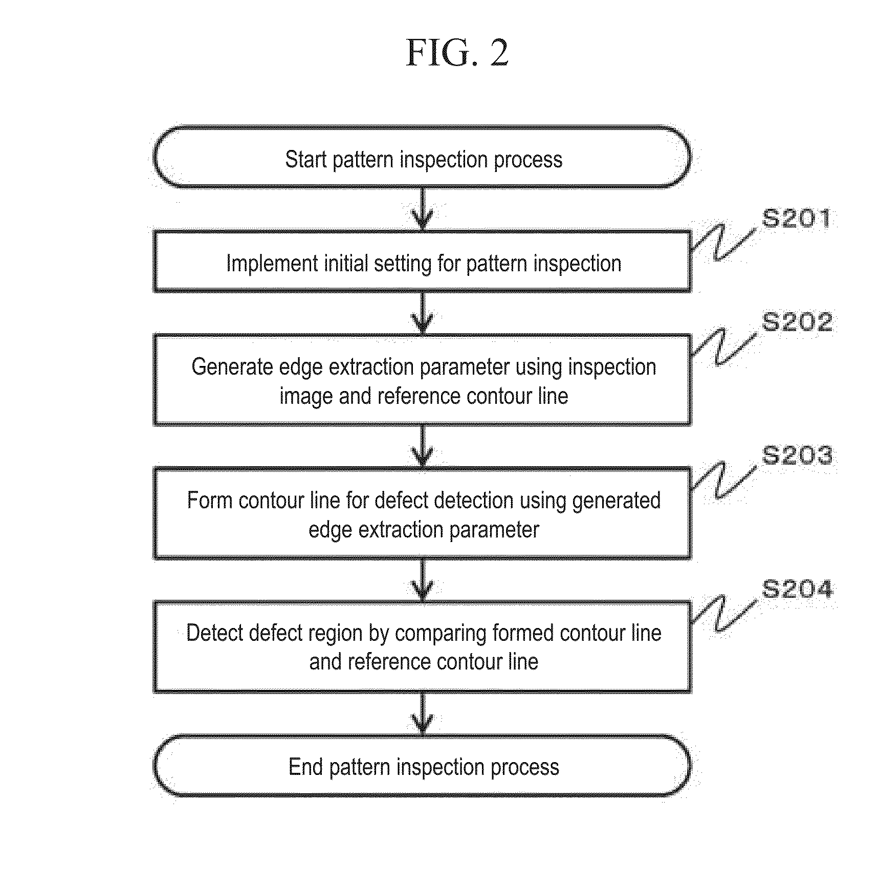
[0065]In the following, a first embodiment will be described with reference to FIG. 1 to FIG. 16. The present embodiment is an example of a pattern inspecting device which may be suitably used for extracting, by inspection involving image acquisition in a relatively large field of view with respect to the dimension of a pattern as the object of evaluation (image acquisition at low magnification ratio), a pattern region or a “defect region” (region with high risk of defect development) which is locally deformed with respect to a contour shape given in advance as an inspection reference.

[0066]As the semiconductor process rule evolves and increasingly finer patterns are transferred on a wafer, there is a growing need for inspection using design data so as to detect systematic defect caused by mask design flaw and the like. This is because, in addition to a decrease in the margin for parameter setting for mask design or transfer, making it easier for systematic defect to...

second example

Second Embodiment

[0223]In the following, a second embodiment will be described with reference to FIG. 26 to FIG. 30. The present embodiment represents an example of a dimension measuring device which may be preferably used for measuring the dimension of the evaluation object pattern while decreasing the influence of noise or the influence of small roughness.

[0224]In the field of semiconductor manufacturing, dimension management has been implemented using a dimension measured from an image obtained by CD-SEM (SEM image), by a threshold value method, for example. The object of dimension management includes, for example, the line pattern width and hole pattern diameter. As the process rule evolves, pattern dimension becomes smaller, and the influence of length measurement value variations accompanying side wall irregularities on the pattern dimension becomes relatively large. As a result, there is a growing need for accurately measuring and managing an index referred to as line edge ro...

third example

Third Embodiment

[0260]In the following, a third embodiment will be described with reference to FIG. 31 to FIG. 34. The present embodiment represents an example of a dimension measuring device which may be preferably used for the purpose of quantifying and evaluating the two-dimensional shape of a measurement object pattern by shape comparison with a reference contour shape. In the case of quality management based on one-dimensional dimension, evaluation can be made by comparison with a reference dimension value. However, in the case of quality management based on two-dimensional shape, it is necessary to evaluate by comparison with the shape of the reference contour line. Normally, evaluation is made by comparison of the shape of a given contour line as an evaluation reference with the shape of a contour line determined from an image obtained by imaging a pattern as the object of evaluation. In this case, there is a problem similar to that of the second embodiment when the contour l...


PUM


Abstract

Provided is a pattern inspecting and measuring device that decreases the influence of noise and the like and increases the reliability of an inspection or measurement result during inspection or measurement using the position of an edge extracted from image data obtained by imaging a pattern as the object of inspection or measurement. For this purpose, in the pattern inspecting and measuring device in which inspection or measurement of an inspection or measurement object pattern is performed using the position of the edge extracted, with the use of an edge extraction parameter, from the image data obtained by imaging the inspection or measurement object pattern, the edge extraction parameter is generated using a reference pattern having a shape as an inspection or measurement reference and the image data.

Description

TECHNICAL FIELD[0001]The present invention relates to a pattern inspecting and measuring device for inspecting or measuring a pattern using the position of an edge of an inspection or measurement object pattern, and a computer program executed by a computer of the pattern inspecting and measuring device.BACKGROUND ART[0002]In the field of semiconductor manufacturing, inspecting devices and measuring devices using a scanning electron microscope (SEM) have long been used.[0003]As increasingly finer patterns are transferred on a wafer with the evolution of process rule, the density of patterns formed on the wafer also becomes higher, increasing the number of locations requiring evaluation by dimension measurement. As a result, from the viewpoint of reducing the evaluation time, there is a growing demand for narrowing the locations where the risk of defect development is high, i.e., measurement points that require evaluation with higher magnification ratios, by an inspection involving i...

Claims


Application Information

Patent Timeline
IPC IPC(8): G06T7/00G06K9/52G06K9/46
CPCG06T7/001G06K9/52G06K9/4604G06T7/13G06T7/0002H01J37/244G01B2210/56G06T2207/30168H01J2237/24592H01J2237/2817
Inventor MINAKAWA, TSUYOSHIHIROI, TAKASHIYOSHIDA, TAKEYUKININOMIYA, TAKUYAMAMOTO, TAKUMASHINDO, HIROYUKIFUKUNAGA, FUMIHIKOTOYODA, YASUTAKASHINODA, SHINICHI
Owner HITACHI HIGH-TECH CORP
Why Eureka
Try Eureka