Semiconductor device

Active Publication Date: 2015-08-20
LONGITUDE LICENSING LTD
View PDF5 Cites 2 Cited by
  • Summary
  • Abstract
  • Description
  • Claims
  • Application Information

AI Technical Summary

Benefits of technology

The present invention allows for the clean control of power-supply noise and the rapid and continuous switching of impedance through the use of multiple unit buffers. This means that the peak current flow during output is dispersed, resulting in more effective and controlled power-supply noise control.

Problems solved by technology

However, with the semiconductor devices described in patent literature articles 1 and 2, because the selected unit buffers are activated simultaneously, the peak current that flows during the output operation increases as the number of activated unit buffers increases, and significant power-supply noise is sometimes generated.
However, with the semiconductor device described in patent literature article 3, because a binary-format weighting is applied to the impedance of each buffer, it is necessary to switch the value of a binary-format signal very rapidly and continuously in order to create an arbitrary waveform, and this is not practical for high-speed data transfer.

Method used


Image

  • Semiconductor device
  • Semiconductor device
  • Semiconductor device

Examples


Embodiment Construction

[0053]Preferred modes of embodiment of the present invention will now be described in detail with reference to the accompanying drawings.

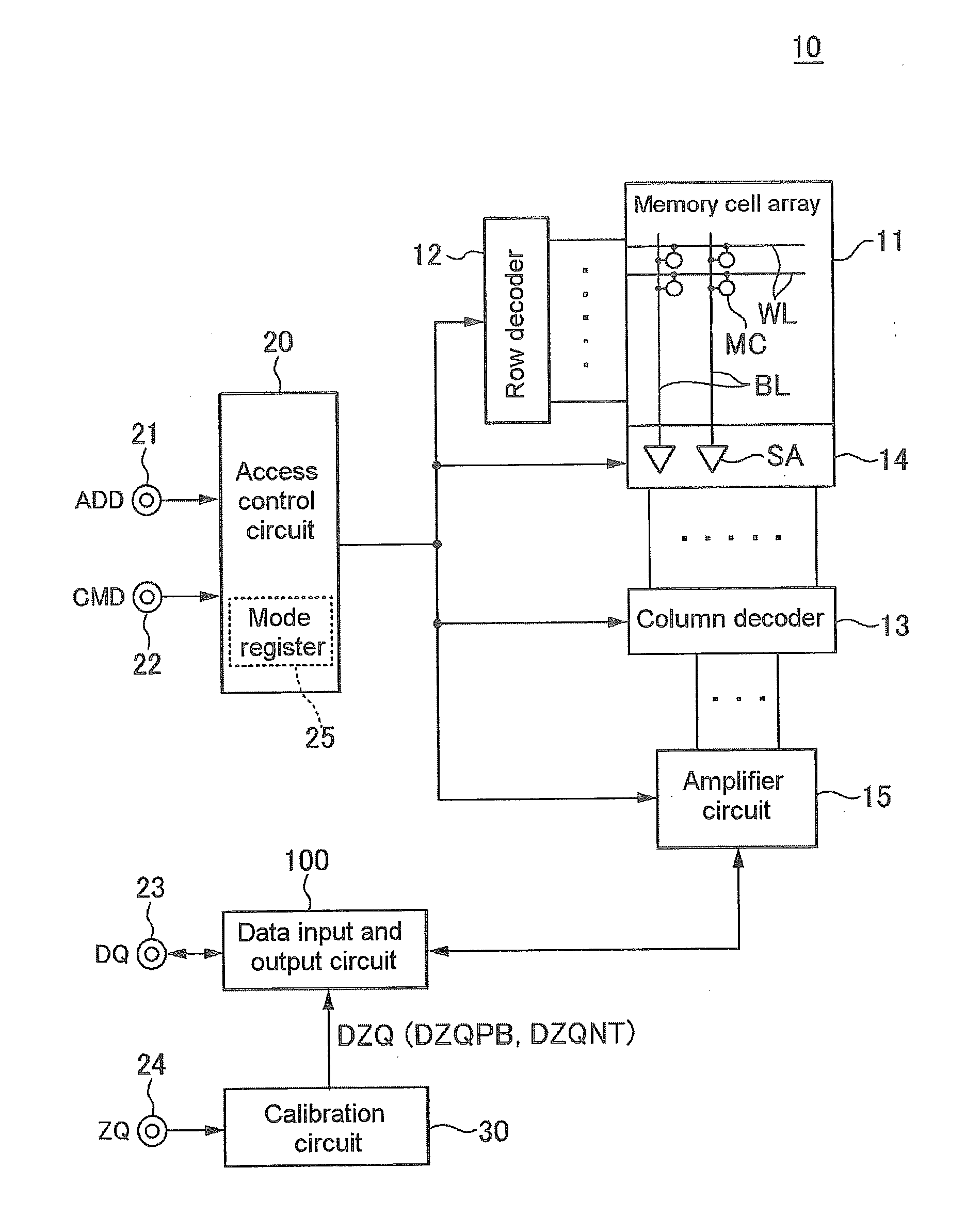
[0054]FIG. 1 is a block diagram illustrating the overall configuration of a semiconductor device 10 according to a preferred mode of embodiment of the present invention.

[0055]The semiconductor device 10 according to this mode of embodiment is a DRAM, and as illustrated in FIG. 1 it is provided with a memory cell array 11. The memory cell array 11 is provided with a plurality of word lines WL and a plurality of bit lines BL which intersect each other, and memory cells MC are disposed at the points of intersection. The word lines WL are selected using a row decoder 12, and the bit lines BL are selected using a column decoder 13. The bit lines BL are connected respectively to corresponding sense amplifiers SA in a sensing circuit 14, and the bit lines BL selected by the column decoder 13 are connected to an amplifier circuit 15 by way of the sense amp...


PUM


Abstract

A semiconductor device includes data terminal, unit buffers which drive the data terminal and the impedance of which can be adjusted, and control circuits which successively switch the operation of at least two unit buffers selected from unit buffers. Because the operation of the plurality of unit buffers is switched successively, the peak current which flows during an output operation is dispersed, power-supply noise can be controlled, and the output potential can be switched very rapidly and continuously, while a fixed output impedance is maintained.

Description

TECHNICAL FIELD[0001]The present invention relates to a semiconductor device, and in particular relates to a semiconductor device provided with a plurality of unit buffers connected in parallel to data terminals.BACKGROUND ART[0002]Semiconductor devices such as DRAM (Dynamic Random Access Memory) are sometimes configured in such a way that the impedance of an output buffer circuit can be switched according to an operating mode. For example in semiconductor devices described in patent literature articles 1 and 2, an output buffer circuit is configured from a plurality of unit buffers having the same impedance as each other, and the impedance can be switched by selecting the number of unit buffers to activate. With the semiconductor devices described in patent literature articles 1 and 2, because each unit buffer has the same impedance, a calibration operation to adjust the impedance of the unit buffers can be executed in one batch.PRIOR ART LITERATUREPatent Literature[0003]Patent lit...

Claims


Application Information

Patent Timeline
IPC IPC(8): G11C7/10
CPCG11C7/1057H03K19/0175
Inventor ARAI, TETSUYAASAKI, KENJI
Owner LONGITUDE LICENSING LTD
Why Eureka
Try Eureka