Output Buffer Circuit Capable of Enhancing Stability

Active Publication Date: 2011-08-04
NOVATEK MICROELECTRONICS CORP
View PDF4 Cites 13 Cited by
  • Summary
  • Abstract
  • Description
  • Claims
  • Application Information

AI Technical Summary

Benefits of technology

[0008]It is therefore an objective of the claimed invention to provide an output buffer circuit capable of enhancing stability.
[0009]The present invention discloses an output buffer circuit capable of enhancing stability. The output buffer circuit includes an operational amplifier, a capacitive load, and an output control unit. The operational amplifier has a positive input terminal, a negative input terminal and an output terminal reversely coupled to the negative input terminal, and is utilized for generating

Problems solved by technology

However, in order to decrease power loss, the conventional source driver continuously reduces the DC currents of the output buffer, causing that a phase margin of the operational amplifier is

Method used


Image

  • Output Buffer Circuit Capable of Enhancing Stability
  • Output Buffer Circuit Capable of Enhancing Stability
  • Output Buffer Circuit Capable of Enhancing Stability

Examples


Example

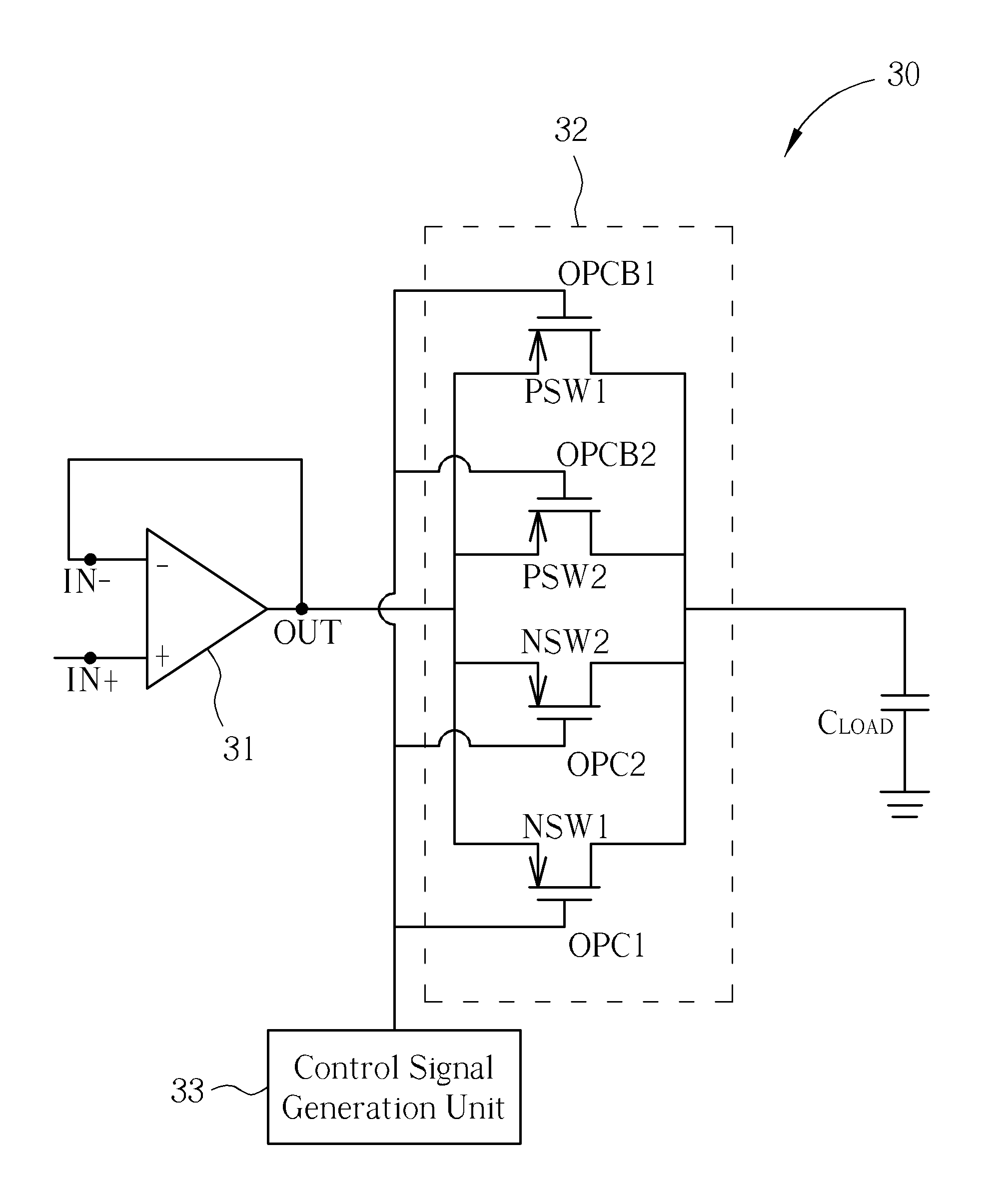
[0018]Please refer to FIG. 3, which is a schematic diagram of an output buffer circuit 30 according to the embodiment of the present invention. The output buffer circuit 30 includes an operational amplifier 31, a capacitive load CLOAD and an output control unit 32. The operational amplifier 31 has a positive input terminal IN+, a negative input terminal IN−, and an output terminal OUT. The positive input terminal IN+ is utilized for receiving an analog voltage; The output terminal OUTPUT is coupled to the negative input terminal IN− to form a negative feedback loop. The operational amplifier 31 generates a corresponding output voltage to the output terminal OUT according to the analog voltage received by the positive input terminal IN+. The output control unit 32, coupled between the output terminal OUT of the operational amplifier 31 and the capacitive load CLOAD, is utilized for controlling electrical connection between the output terminal OUT of the operational amplifier 31 and t...


PUM


Abstract

An output buffer circuit capable of enhancing stability includes an operational amplifier, a capacitive load and an output control unit. The operational amplifier has a positive input terminal, a negative input terminal and an output terminal, and generates an output voltage to the output terminal according to an input voltage received by the positive input terminal. The output control unit is coupled between the output terminal of the operational amplifier and the capacitive load, and is utilized for controlling electrical connection between the output terminal of the operational amplifier and the capacitive load to forma signal output path and for adjusting impedance of the signal output path when the signal output path is formed.

Description

BACKGROUND OF THE INVENTION[0001]1. Field of the Invention[0002]The present invention relates to an output buffer circuit capable of enhancing stability, and more particularly to an output buffer circuit that increases a phase margin of an operational amplifier by adjusting output path impedance of the operational amplifier.[0003]2. Description of the Prior Art[0004]Output buffers are usually applied to various electronic devices for isolating signals from input terminals to output terminals to avoid the input terminals being affected by loading and for enhancing driving ability. In Liquid Crystal Display (LCD) devices, for example, source drivers charge each pixel in LCD panels to an individual voltage level to drive liquid crystal molecules of each pixel by using the output buffers. Hence, the driving ability of the output buffer is highly related to display performance and responding time of the LCD devices.[0005]Please refer to FIG. 1, which is a schematic diagram of a conventio...

Claims


Application Information

Patent Timeline
IPC IPC(8): H03F1/56
CPCH03F1/34H03F1/56G09G2310/0291G09G3/3688G09G3/3685
Inventor HSU, XIE-RENCHEN, JI-TINGKUO, YAO-HUNG
Owner NOVATEK MICROELECTRONICS CORP
Why Eureka
Try Eureka