

Pixel structure and display panel
- Summary
- Abstract
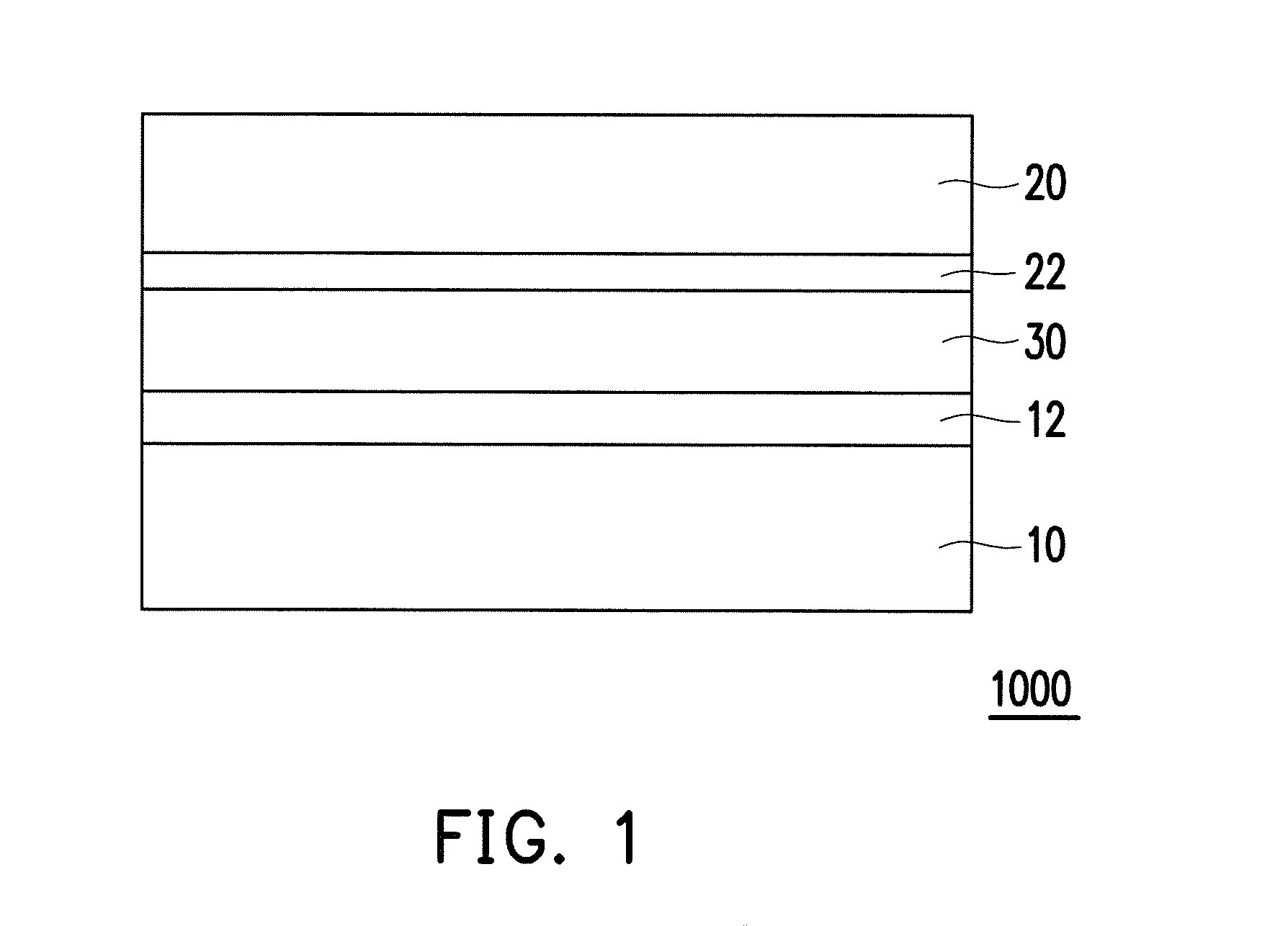
- Description
- Claims
- Application Information
AI Technical Summary
Benefits of technology
Problems solved by technology
Method used
Image

Examples
first embodiment
[0069]FIG. 3 is a schematic top view illustrating a pixel electrode in a pixel structure according to the disclosure. FIG. 4 is a schematic top view illustrating a passivation layer below the pixel electrode depicted in FIG. 3. FIG. 5 is a schematic view illustrating that the pixel electrode depicted in FIG. 3 and the passivation layer depicted in FIG. 4 are overlapped. With reference to FIG. 3, the pixel electrode 120 has at least one block-shaped electrode (i.e., at least one plate electrode) 122 and a plurality of first branch electrodes 124. Particularly, the block-shaped electrode 122 is an electrode region in the pixel electrode 120 and is not patterned; that is, the block-shaped electrode 122 does not have any opening, hole, slit, groove, and gap. By contrast, the first branch electrodes 124 are electrode regions in the pixel electrode 120 and are patterned. The pixel electrode 120 may further include a main electrode (i.e., a main-truck electrode) 126. The first branch elect...
second embodiment
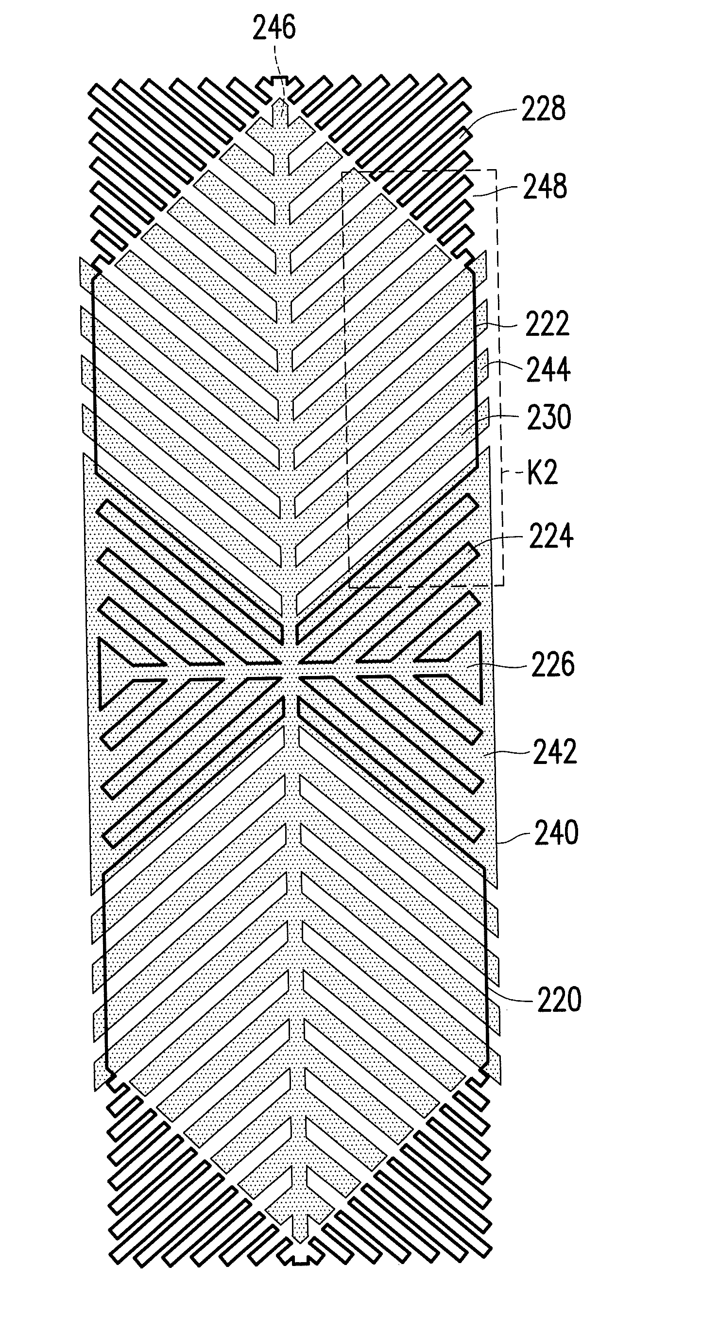
[0077]FIG. 9 is a schematic top view illustrating a pixel electrode in a pixel structure according to the disclosure. FIG. 10 is a schematic top view illustrating a passivation layer below the pixel electrode depicted in FIG. 9. FIG. 11 is a schematic view illustrating that the pixel electrode depicted in FIG. 9 and the passivation layer depicted in FIG. 10 are overlapped. As shown in FIG. 9, the pixel electrode 220 has at least one block-shaped electrode (i.e., at least one plate electrode) 222, a plurality of first branch electrodes 224, a main electrode (i.e., a main-truck electrode) 226, and a plurality of outer branch electrodes 228. Particularly, the block-shaped electrode 222 is an electrode region in the pixel electrode 220 and is not patterned; that is, the block-shaped electrode 222 does not have any opening, hole, slit, groove, and gap. By contrast, the first branch electrodes 224, the main electrode 226, and the outer branch electrodes 228 are electrode regions in the pi...
third embodiment
[0083]FIG. 13 is a schematic top view illustrating a pixel electrode in a pixel structure according to the disclosure. FIG. 14 is a schematic top view illustrating a passivation layer below the pixel electrode depicted in FIG. 13. FIG. 15 is a schematic view illustrating that the pixel electrode depicted in FIG. 13 and the passivation layer depicted in FIG. 14 are overlapped. As shown in FIG. 13, the pixel electrode 320 has at least one block-shaped electrode (i.e., at least one plate electrode) 322, a plurality of first branch electrodes 324, a first main electrode (i.e., a first main-truck electrode) 326, and a second main electrode (i.e., a second main-truck electrode) 328. Particularly, the block-shaped electrode 322 is an electrode region in the pixel electrode 320 and is not patterned; that is, the block-shaped electrode 322 does not have any opening, hole, slit, groove, and gap. By contrast, the first branch electrodes 324 are electrode regions in the pixel electrode 320 and ...
PUM
 Abstract
Description
Claims
Application Information