TFT and Manufacturing Method Thereof, Array Substrate and Display Device

a technology of thin film transistor and array substrate, applied in the field of thin film transistor, can solve the problems of low carrier mobility of active layer made of a-si, difficult to meet the requirements of some high-performance display devices, and relatively small channel current, so as to achieve low process complexity, effective channel current, and low carrier mobility

Active Publication Date: 2015-08-27
BOE TECH GRP CO LTD +1
View PDF4 Cites 2 Cited by
  • Summary
  • Abstract
  • Description
  • Claims
  • Application Information

AI Technical Summary

Benefits of technology

[0004]Accordingly, an object of the present invention is to provide a thin film transistor and a manufacturing method thereof, and an array substrate, in order to increase the channel current of an active layer in the thin film transistor.
[0020]For example, the step of alternately depositing a plurality of active semiconductor film layers and a plurality of insulation film layers comprises: by controlling the deposition pressure and the gas flow, allowing the compactness of the plurality of active semiconductor film layers and the plurality of insulation film layers to gradually become larger from top to bottom in the thickness direction of the active layer.
[0028]It can be seen that, by forming a plurality of active semiconductor sub-layers and insulation sub-layers which are stacked alternately in a thin film transistor, the present invention may form multiple channels in the thin film transistor, so that the channel current may be increased effectively, and the problem of small channel current resulted from low carrier mobility of the active layer may be solved. Compared with the prior art, the present invention is relatively low in process complexity and may effectively save cost.

Problems solved by technology

However, the active layer made of a-Si:H has low carrier mobility.
Because there are many defects in a-Si:H, most charges attracted by a gate in a TFT array substrate are captured in the defects and cannot conduct electricity, so that the carrier mobility of the active layer is less than 1 cm2 / (V*s), thus the channel current is relatively small, and it is difficult to meet the requirements of some high-performance display devices.
However, the low-temperature polycrystalline silicon is complicated in manufacturing process, high in manufacturing cost and poor in homogeneity and stability, comprehensive and stable crystallization of the low-temperature polycrystalline silicon is difficult to be realized, while the amorphous IGZO is high in manufacturing cost, immature in manufacturing process and low in yield.

Method used


Image

  • TFT and Manufacturing Method Thereof, Array Substrate and Display Device
  • TFT and Manufacturing Method Thereof, Array Substrate and Display Device
  • TFT and Manufacturing Method Thereof, Array Substrate and Display Device

Examples


Embodiment Construction

[0036]The specific embodiments of the present invention will be described as below in details with reference to accompanying drawings. It will be appreciated that the specific embodiments described herein are used for describing and explaining the present invention merely, but are not intended to limit the present invention.

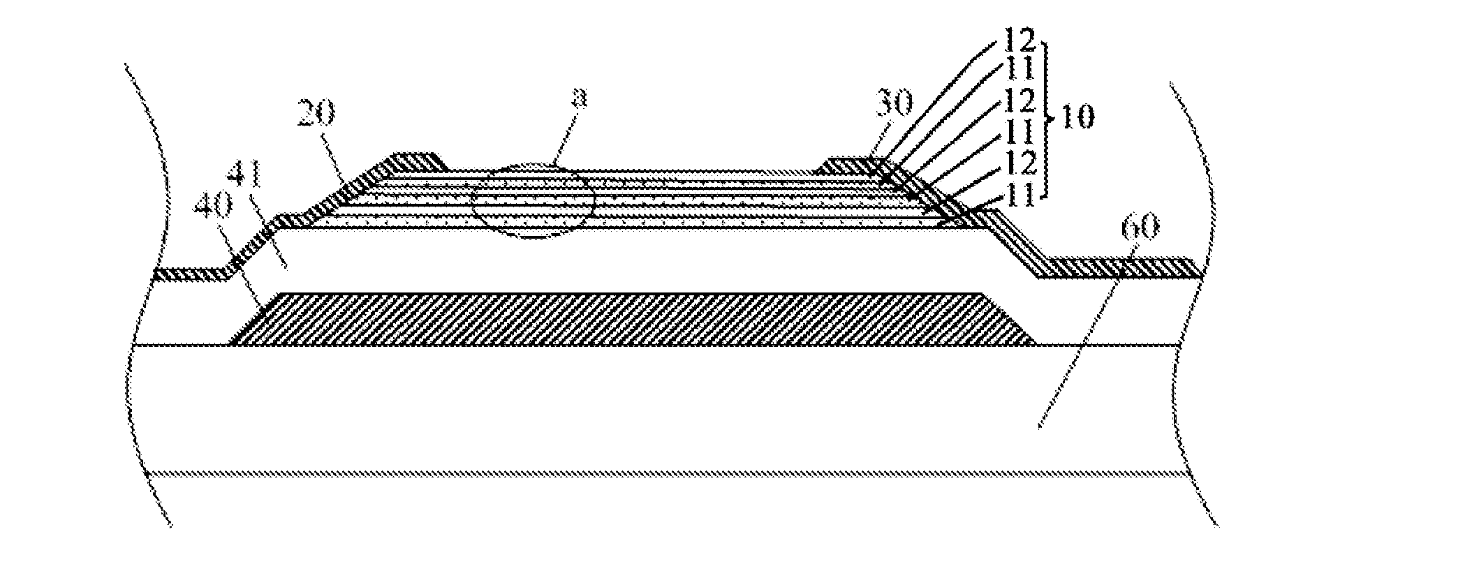
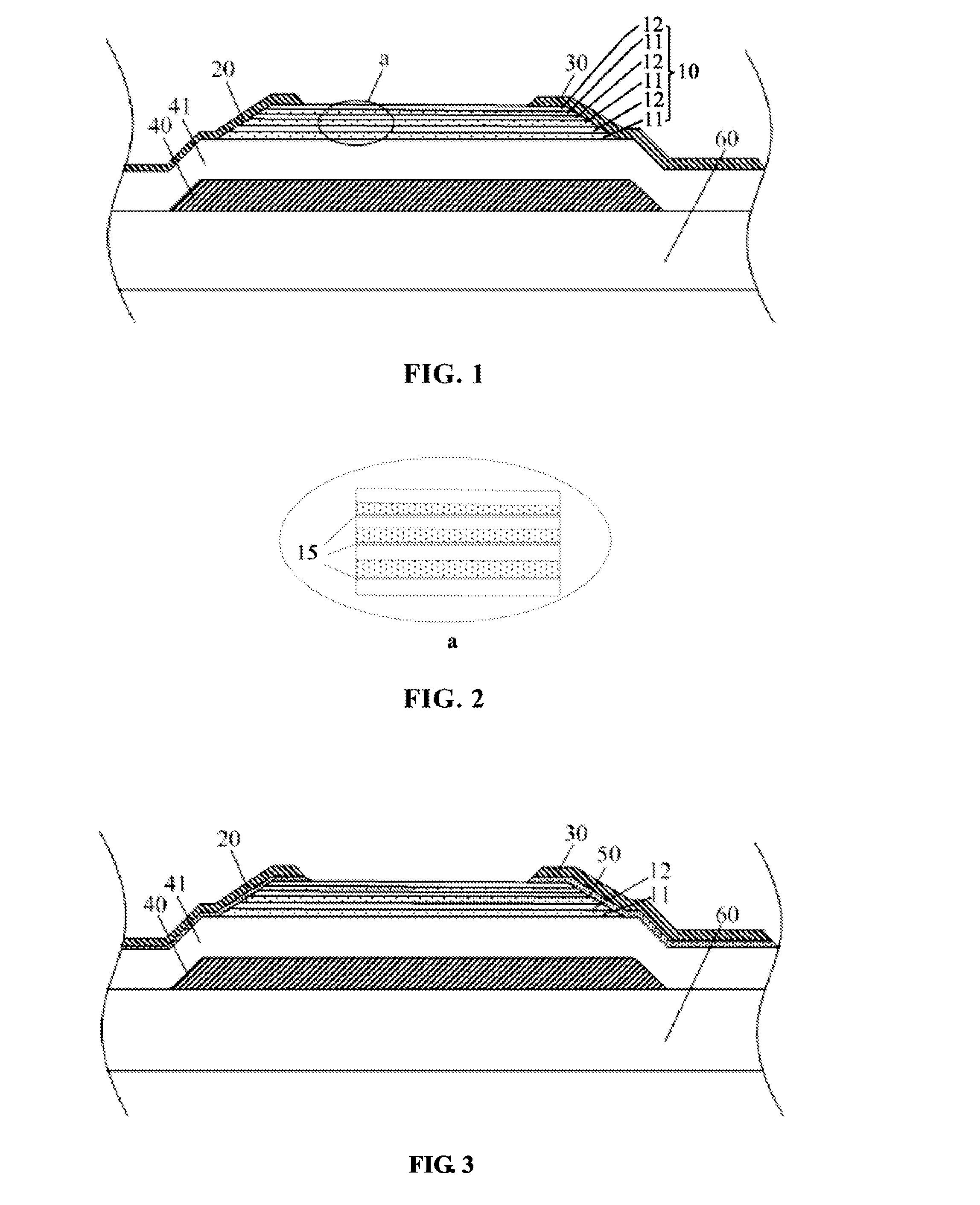
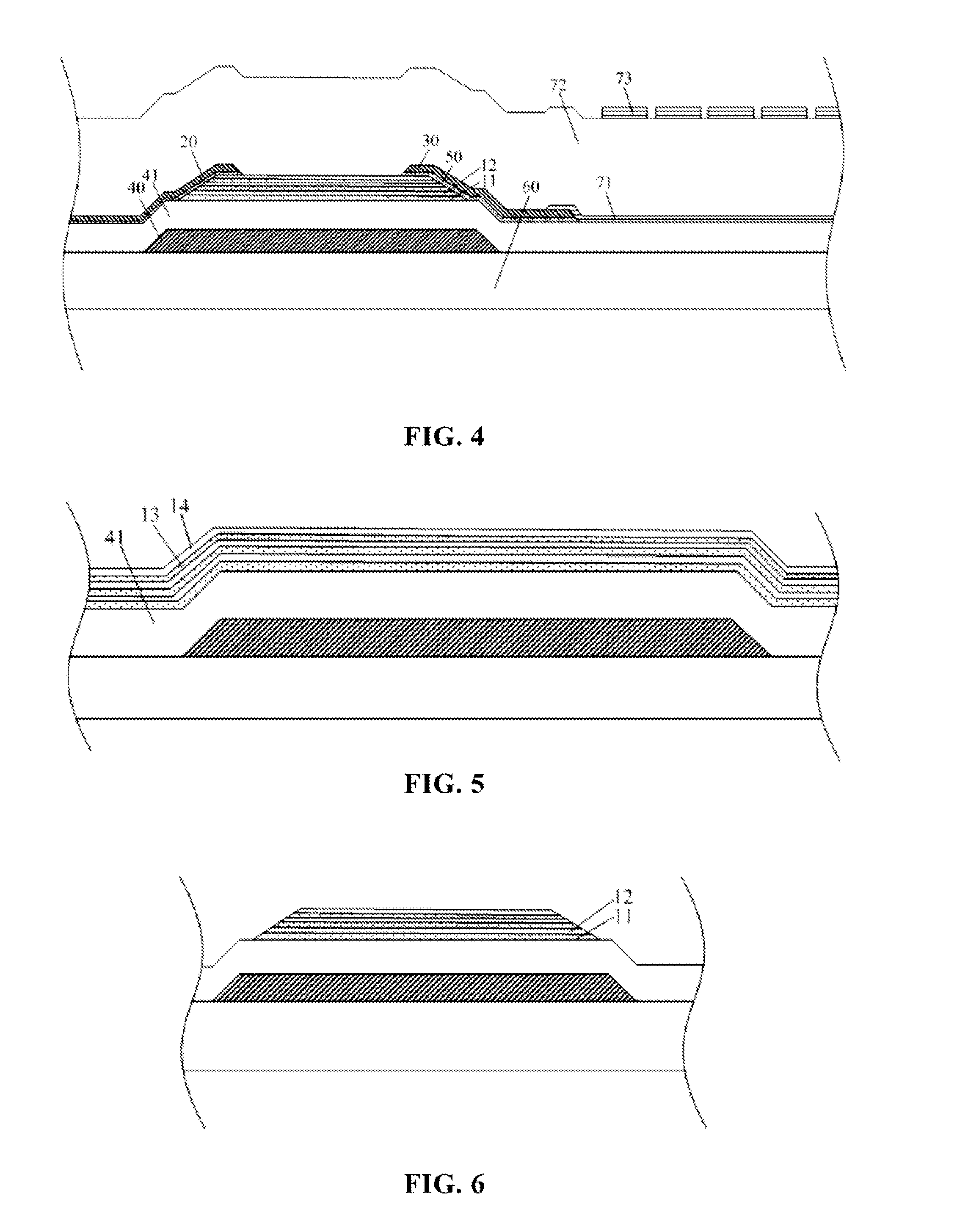
[0037]In one aspect of the present invention, a thin film transistor is provided. As shown in FIG. 1, an active layer 10 of the thin film transistor may comprise a plurality of active semiconductor sub-layers 11 and a plurality of insulation sub-layers 12, which are stacked alternately. A source 20 and a drain 30 of the thin film transistor may be electrically connected to the plurality of active semiconductor sub-layers 11.

[0038]Specifically, as shown in FIG. 1, the thin film transistor may comprise a base substrate 60, and a gate 40 and a gate insulation layer 41 formed on the base substrate 60. The active layer 10 may be formed on the gate insulation layer 41,...


PUM


Abstract

The present invention provides a thin film transistor. An active layer of the thin film transistor comprises a plurality of active semiconductor sub-layers and a plurality of insulation sub-layers, which are stacked alternately. A source and a drain of the thin film transistor are electrically connected to the plurality of active semiconductor sub-layers. Correspondingly, the present invention further provides a method for manufacturing a thin film transistor, and an array substrate. The present invention can effectively increase channel current of the active layer in a thin film transistor, and solves the problem of small channel current resulted from low carrier mobility of the active layer.

Description

FIELD OF THE INVENTION[0001]The present invention relates to the field of display technology, and particularly to a thin film transistor and a manufacturing method thereof, an array substrate and a display device.BACKGROUND OF THE INVENTION[0002]In an existing TFT (Thin Film Transistor) array substrate, an active layer of a thin film transistor is usually made of hydrogenated amorphous silicon (a-Si:H). a-Si:H has advantages of good homogeneity, the capability of large-area deposition, good thin film stability, etc. However, the active layer made of a-Si:H has low carrier mobility. Because there are many defects in a-Si:H, most charges attracted by a gate in a TFT array substrate are captured in the defects and cannot conduct electricity, so that the carrier mobility of the active layer is less than 1 cm2 / (V*s), thus the channel current is relatively small, and it is difficult to meet the requirements of some high-performance display devices.[0003]In the existing methods, an active ...

Claims


Application Information

Patent Timeline
Patent Type & Authority Applications(United States)
IPC IPC(8): H01L27/12H01L29/786H01L21/47H01L29/66
CPCH01L27/124H01L21/47H01L29/78669H01L29/66765H01L27/1214H01L29/45H01L29/6675H01L29/78663
Inventor ZHANG, JINZHONG
Owner BOE TECH GRP CO LTD
Why Eureka
Try Eureka