Dual-grid three-dimensional storage device and fabrication method thereof

A manufacturing method and memory technology, applied in the field of flash memory, can solve problems such as doping fluctuations of storage devices, affecting device performance, and threshold voltage interference, and achieve the effects of avoiding threshold voltage interference, improving current channels, and increasing memory cell density

Active Publication Date: 2018-03-13
YANGTZE MEMORY TECH CO LTD
View PDF5 Cites 0 Cited by
  • Summary
  • Abstract
  • Description
  • Claims
  • Application Information

AI Technical Summary

Problems solved by technology

However, the inventors found that the existing memory structure needs to occupy more memory cells because it includes two TSGs. In addition, the implantation of high-concentration boron will lead to random doping fluctuations in the memory device, which further leads to threshold voltage interference. , in addition, there will be a large threshold voltage swing between the two TSGs, which will affect the performance of the device

Method used


Image

  • Dual-grid three-dimensional storage device and fabrication method thereof
  • Dual-grid three-dimensional storage device and fabrication method thereof
  • Dual-grid three-dimensional storage device and fabrication method thereof

Examples


Embodiment Construction

[0035] The following will clearly and completely describe the technical solutions in the embodiments of the present invention with reference to the accompanying drawings in the embodiments of the present invention. Obviously, the described embodiments are only some, not all, embodiments of the present invention. Based on the embodiments of the present invention, all other embodiments obtained by persons of ordinary skill in the art without making creative efforts belong to the protection scope of the present invention.

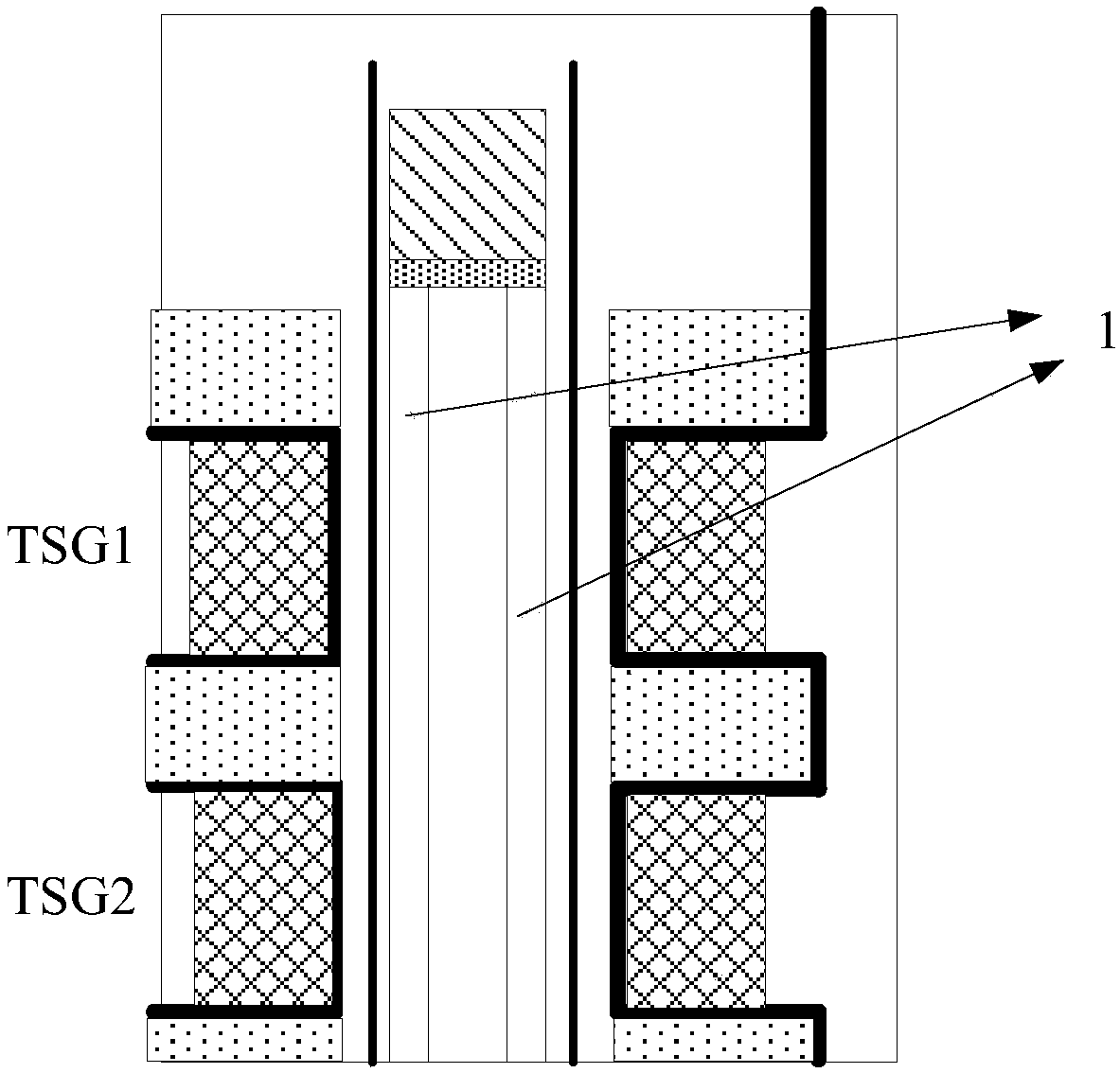
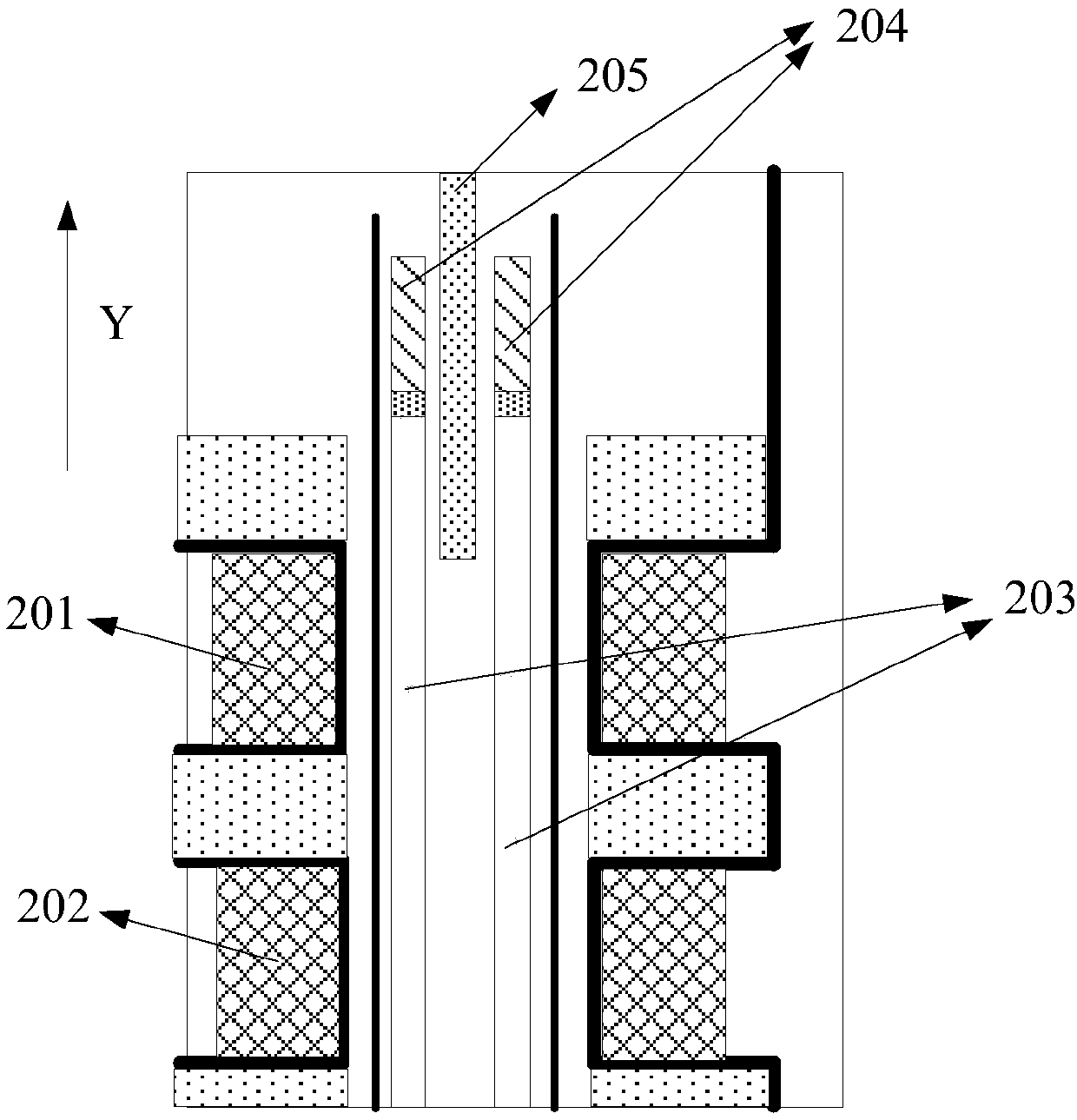
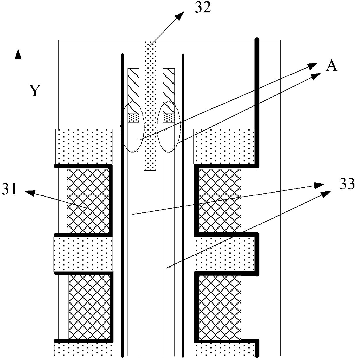
[0036] A double-gate three-dimensional memory and its manufacturing method, the three-dimensional memory includes: TSG and memory cells, and two channels are opened in the three-dimensional memory, and a doping plug is formed on each of the channels, A gate structure is arranged between the two doped plugs, and the gate structure insulates the two doped plugs from each other. It can be seen that in this solution, there is a doped plug on each channel, so the c...


PUM


Abstract

The embodiment of the invention provides a dual-grid three-dimensional storage device and a fabrication method thereof. The three-dimensional storage device comprises a TSG and a storage unit, whereintwo channels are formed in the three-dimensional storage device, a doping plug is formed on each channel, a grid structure is arranged between the two doping plugs, and the doping plugs are isolatedby the grid structure. In the three-dimensional storage device, the doping plug is arranged on each channel, thus, the current resistance can be reduced, and the current passage is improved; by increasing the number of the doping plug, only a TSG is needed, and the problem of excessively large threshold voltage amplitude generated between two TSGs is prevented; the current passage is improved, thus, no boron is injected into the channels, and the problem of threshold value interference generated by the storage device caused by high-concentration doping is further prevented; and moreover, sincethe three-dimensional storage device only comprises the TSG, the density of the storage unit can be improved.

Description

technical field [0001] The invention relates to the field of flash memory, and more specifically, to a double-gate three-dimensional memory and a manufacturing method thereof. Background technique [0002] NAND flash memory is a better storage device than hard disk drives, and it has been widely used in electronic products as people pursue non-volatile storage products with low power consumption, light weight and high performance. At present, the planar NAND flash memory is close to the limit of practical expansion. In order to further increase the storage capacity and reduce the storage cost per bit, a 3D NAND memory is proposed. [0003] In the 3D NAND memory structure, in order to increase the current while reducing the bit line current, usually, the top gate structure is designed as figure 1 In the structure shown, the 3D NAND memory structure includes two TSGs (TSG1 and TSG2) in the same bit line, and in order to increase the threshold voltage between the two TSGs, bor...

Claims


Application Information

Patent Timeline
Patent Type & Authority Applications(China)
IPC IPC(8): H01L27/11524H01L27/11551H01L27/1157H01L27/11578
CPCH10B41/20H10B41/35H10B43/20H10B43/35
Inventor 靳磊杨陈辰姜丹丹霍宗亮邹兴奇张易张瑜
Owner YANGTZE MEMORY TECH CO LTD
Why Eureka
Try Eureka