Stacked die integrated circuit

Active Publication Date: 2015-09-24
INVENSAS CORP
View PDF2 Cites 50 Cited by
  • Summary
  • Abstract
  • Description
  • Claims
  • Application Information

AI Technical Summary

Problems solved by technology

However, there are issues associated with forming such “3D ICs”, including without limitation cost.

Method used


Image

  • Stacked die integrated circuit
  • Stacked die integrated circuit
  • Stacked die integrated circuit

Examples


Embodiment Construction

[0020]In the following description, numerous specific details are set forth to provide a more thorough description of the specific examples described herein. It should be apparent, however, to one skilled in the art, that one or more other examples or variations of these examples may be practiced without all the specific details given below. In other instances, well known features have not been described in detail so as not to obscure the description of the examples herein. For ease of illustration, the same number labels are used in different diagrams to refer to the same items; however, in alternative examples the items may be different.

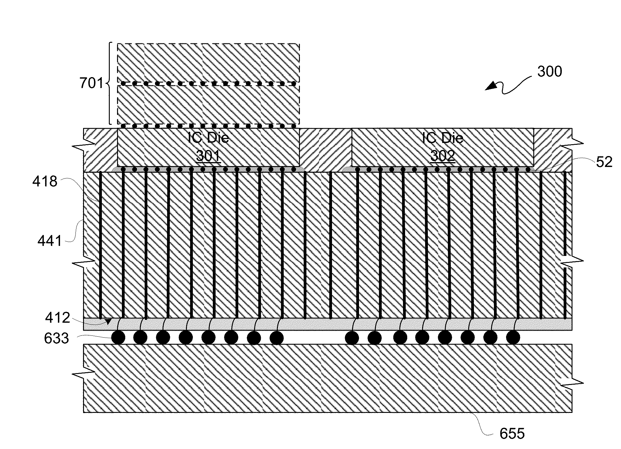
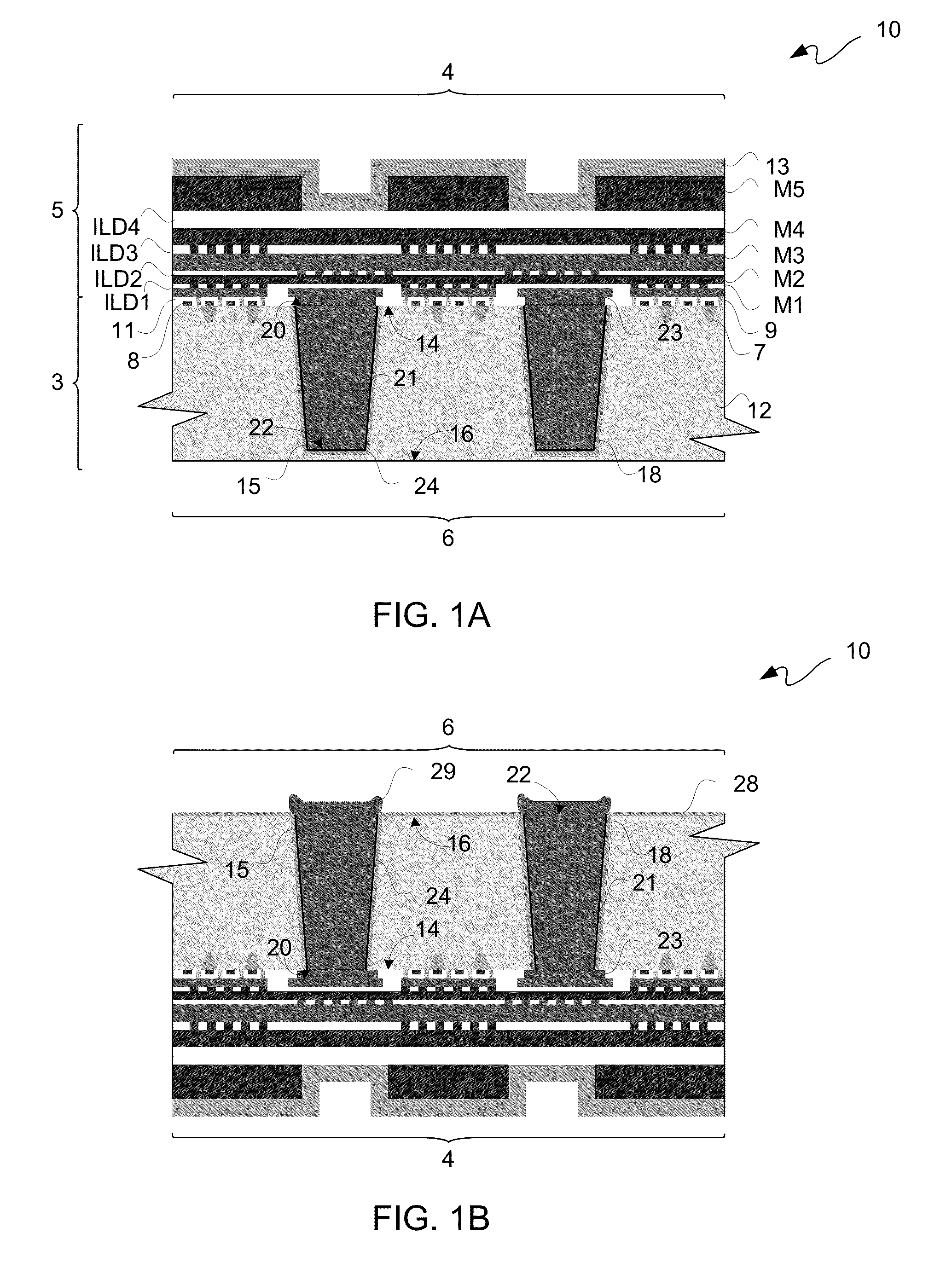
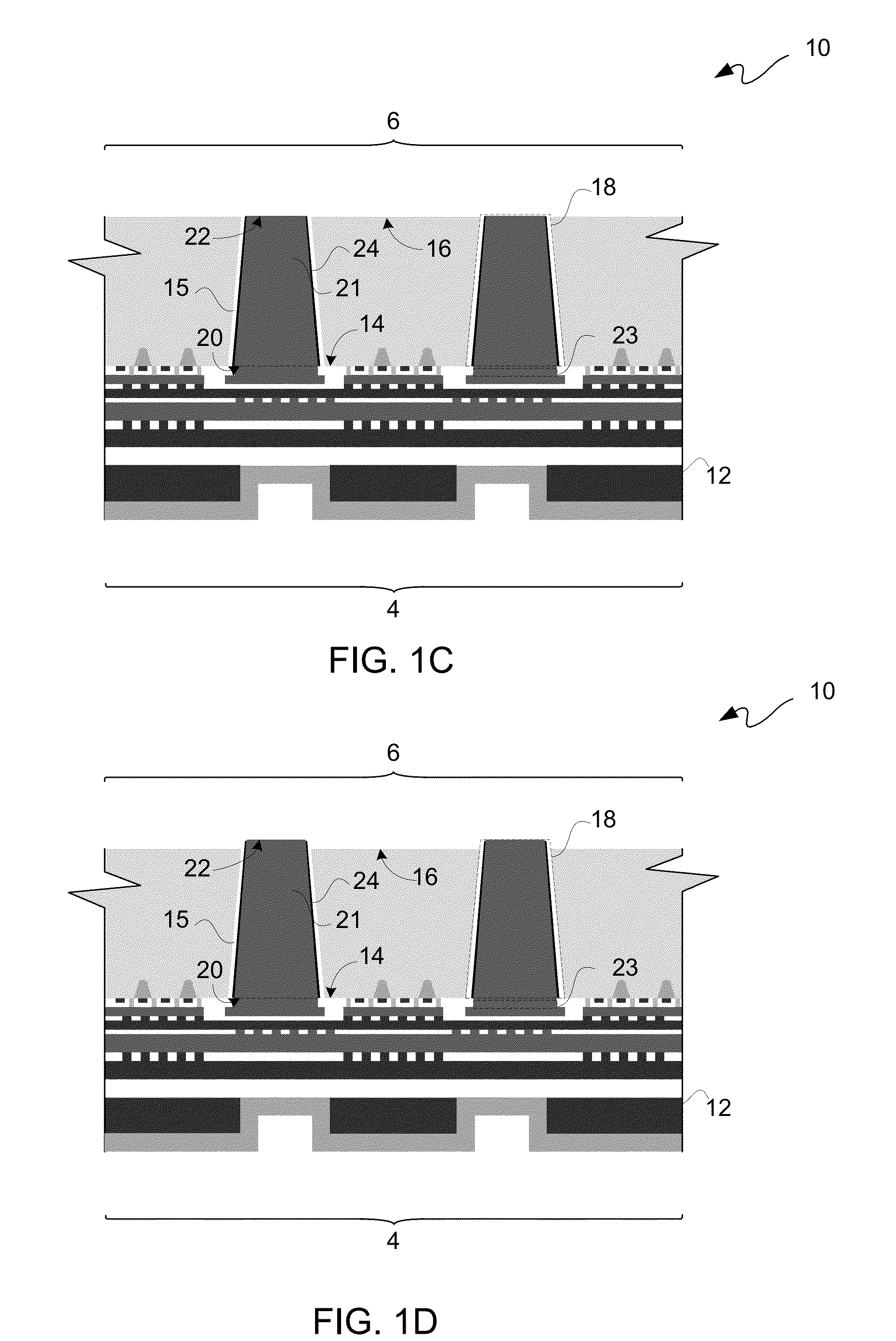
[0021]FIG. 1A is a schematic diagram of a cross-sectional view depicting an exemplary portion of an in-process wafer for providing an IC 10 component. IC 10 includes a substrate 12 of a semiconductor material such as silicon (Si), gallium arsenide (GaAs), polymeric, ceramic, carbon-based substrates such as diamond, a silicon carbon (SiC), germanium...


PUM


Abstract

An apparatus relates generally to an integrated circuit package. In such an apparatus, a package substrate has a first plurality of via structures extending from a lower surface of the package substrate to an upper surface of the package substrate. An die has a second plurality of via structures extending to a lower surface of the die. The lower surface of the die faces the upper surface of the package substrate in the integrated circuit package. The package substrate does not include a redistribution layer. The die and the package substrate are coupled to one another.

Description

FIELD[0001]The following description relates to integrated circuits (“ICs”). More particularly, the following description relates to a stacked die IC.BACKGROUND[0002]Microelectronic assemblies generally include one or more ICs, such as for example one or more packaged dies (“chips”) or one or more dies. One or more of such ICs may be mounted on a circuit platform, such as a wafer such as in wafer-level-packaging (“WLP”), a printed board (“PB”), a printed wiring board (“PWB”), a printed circuit board (“PCB”), a printed wiring assembly (“PWA”), a printed circuit assembly (“PCA”), a package substrate, an interposer, or a chip carrier. Additionally, one IC may be mounted on another IC. An interposer may be an IC, and an interposer may be a passive or an active IC, where the latter includes one or more active devices, such as transistors for example, and the former does not include any active device. Furthermore, an interposer may be formed like a PWB, namely without any circuit elements...

Claims


Application Information

Patent Timeline
Patent Type & Authority Applications(United States)
IPC IPC(8): H01L23/498H01L23/48H01L21/52H01L21/78H01L23/00
CPCH01L23/49827H01L21/78H01L23/481H01L21/52H01L24/85H01L24/94H01L24/97H01L25/0652H01L25/0655H01L2224/13025H01L2224/16225H01L2224/16235H01L2224/1703H01L2224/17181H01L2224/32225H01L2224/32245H01L2224/92125H01L2224/94H01L2224/97H01L2225/06517H01L2225/06589H01L2924/15192H01L2924/15311H01L2924/16251H01L2924/18161H01L2225/06513H01L2225/06541H01L2225/06544H01L2225/06548H01L23/13H01L24/13H01L24/16H01L24/17H01L24/32H01L24/73H01L24/92H01L2224/131H01L2224/13147H01L2224/16145H01L2224/16146H01L2224/16238H01L2224/32145H01L2224/73204H01L2224/73253H01L2924/15159H01L2924/16152H01L2924/16235H01L2924/3511H01L2924/181H01L2924/00014H01L25/0657H01L2224/023H01L2224/83H01L2224/81H01L2924/014H01L2924/0105H01L2924/00H01L2224/45099H01L2924/00012H01L2924/0001H01L21/76898H01L21/304H01L21/4853H01L21/486H01L21/565H01L23/3114H01L23/49838H01L23/49894H01L25/50H01L2225/06555H01L2225/06582
Inventor WOYCHIK, CHARLES G.UZOH, CYPRIAN EMEKAZHANG, RONBUCKMINSTER, DANIELGAO, GUILIAN
Owner INVENSAS CORP
Why Eureka
Try Eureka