
Phase shift circuit, oscillator, electronic apparatus, and moving object
- Summary
- Abstract
- Description
- Claims
- Application Information
AI Technical Summary
Benefits of technology
Problems solved by technology
Method used
Image

Examples
first embodiment
1-1. First embodiment
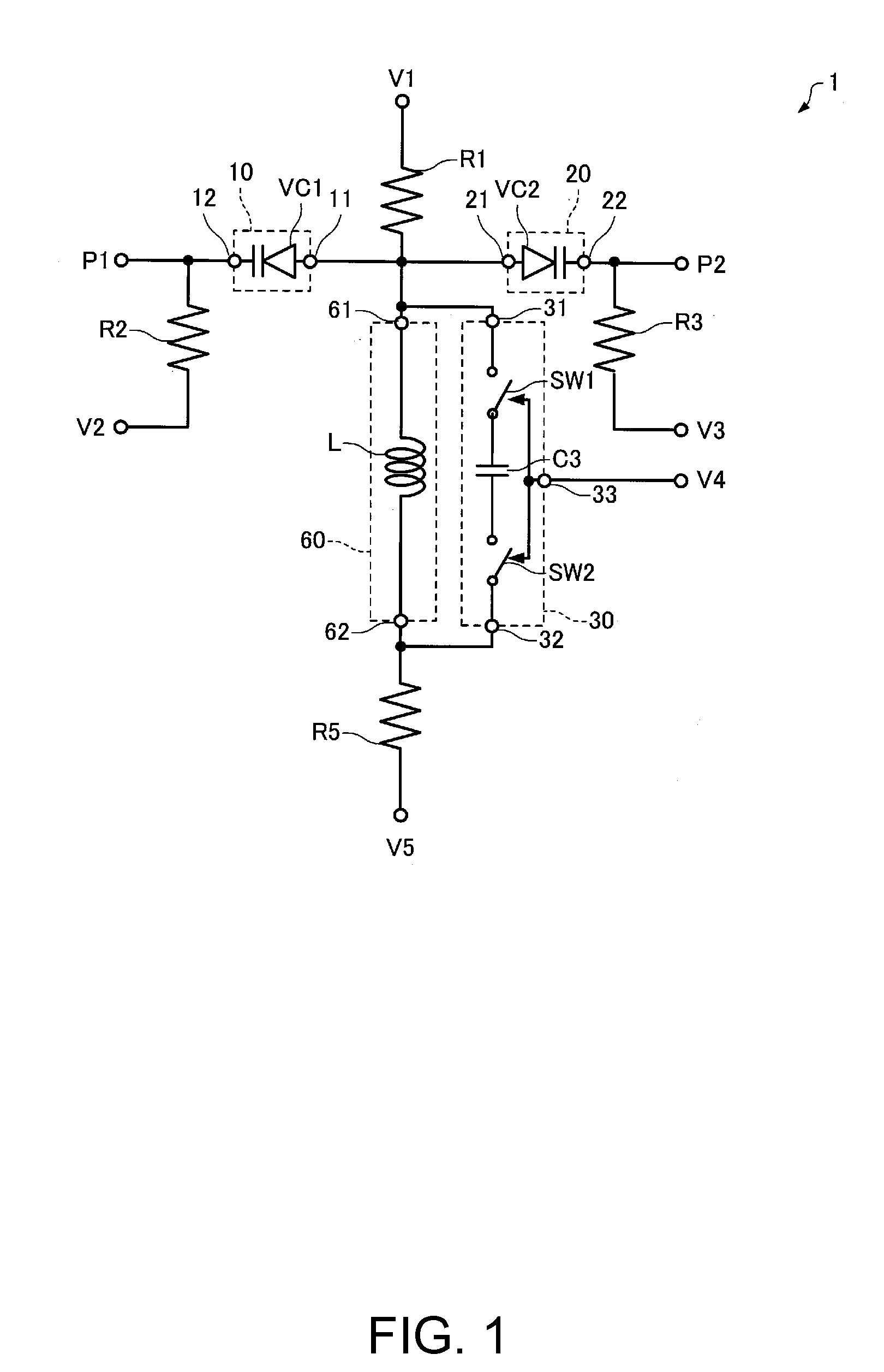
[0049]FIG. 1 is a circuit diagram of a phase shift circuit 1 according to a first embodiment. At least part of the phase shift circuit 1 may be configured as a semiconductor device.
[0050]The phase shift circuit 1 according to the present embodiment includes a first capacitance circuit 10, a second capacitance circuit 20, an inductance circuit 60, and a third capacitance circuit 30, and the third capacitance circuit 30 has a first terminal 31, which is electrically connected to one end (first terminal 61) of the inductance circuit 60, a second terminal 32, which is electrically connected to the other end (second terminal 62) of the inductance circuit 60, and a third terminal 33, to which a signal that controls capacitance is inputted. One end (first terminal 11) of the first capacitance circuit 10, one end (first terminal 21) of the second capacitance circuit 20, the first terminal 31 of the third capacitance circuit 30, and the one end (first terminal 61) of the...
second embodiment
1-2. Second Embodiment
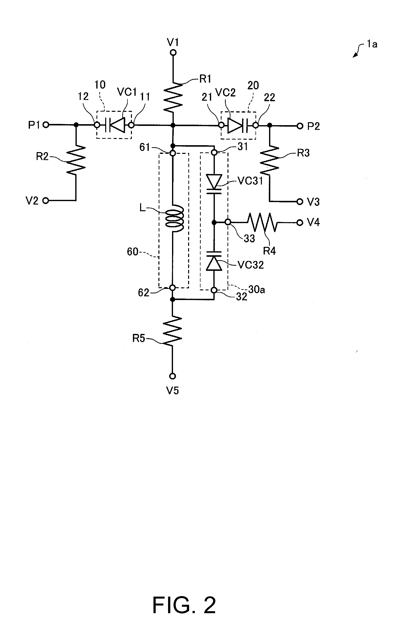
[0064]FIG. 2 is a circuit diagram of a phase shift circuit la according to a second embodiment. The same configurations as those in the phase shift circuit 1 according to the first embodiment have the same reference characters and will not be described in detail.
[0065]In the phase shift circuit la according to the present embodiment, a third capacitance circuit 30a has a variable capacitance circuit in which two variable capacitive elements (variable capacitive element VC31 and variable capacitive element VC32) are connected in series to each other between the first terminal 31 and the second terminal 32, and the third terminal 33 is a connection point where the two variable capacitive elements (variable capacitive element VC31 and variable capacitive element VC32) are connected to each other. In the example shown in FIG. 2, the fourth voltage V4 is applied in the form of a DC voltage to the third terminal 33 via a resistor R4.
[0066]In the example shown in FIG....
third embodiment
1-3. Third Embodiment
[0072]FIG. 3 is a circuit diagram of a phase shift circuit 2 according to a third embodiment. The same configurations as those in the phase shift circuit 1 according to the first embodiment have the same reference characters and will not be described in detail.
[0073]The phase shift circuit 2 according to the present embodiment further includes a fourth capacitance circuit 40 and a fifth capacitance circuit 50, and one end (first terminal 41) of the fourth capacitance circuit 40, one end (first terminal 51) of the fifth capacitance circuit 50, the second terminal 32 of the third capacitance circuit 30, and the second terminal 62 of the inductance circuit 60 are electrically connected to one another.
[0074]The fourth capacitance circuit 40 has a first terminal 41 and a second terminal 42. The fourth capacitance circuit 40 has a capacitive element (capacitor, varicap, or MOS capacitor, for example) between the first terminal 41 and the second terminal 42. The fourth...
PUM
 Abstract
Description
Claims
Application Information