Effective magnetic shield for on-chip inductive structures

a technology of inductive structure and magnetic shield, which is applied in the direction of magnets, inductances, magnetic bodies, etc., can solve the problems of unwanted spurs that can affect the receive sensitivity, coexistence performance, and interference with the transmission mask or regulatory compliance, so as to reduce unwanted magnetic coupling, and increase separation distance

Inactive Publication Date: 2015-10-22
QUALCOMM INC
View PDF3 Cites 28 Cited by
  • Summary
  • Abstract
  • Description
  • Claims
  • Application Information

AI Technical Summary

Benefits of technology

[0006]A magnetic shield for an inductor is disclosed that may substantially reduce unwanted magnetic coupling, compared to conventional shielding techniques, without further sacrificing the performance of the inductor. In accordance with the present embodiments, an inductive apparatus is disclosed that includes an inductor and a magnetic shield to shield the inductor from magnetic coupling effects (e.g., resulting from circuits or components external to the magnetic shield). The magnetic shield includes an inductive ring formed from a plurality of (e.g., at least two) turns surrounding the inductor. Specifically, the effectiveness of the shielding may be directly proportional to the number of turns of the inductive ring, wherein a greater number of turns correlates with a greater reduction in magnetic coupling.
[0009]As described in greater detail below, a magnetic shield that employs a multi-turn inductive ring may significantly reduce unwanted magnetic coupling compared to conventional shielding techniques. Furthermore, by increasing the separation distance between the magnetic shield and the inner inductor, the reductions in magnetic coupling may be achieved without further sacrificing the performance and / or quality of the inductor.

Problems solved by technology

However, due to limitations in chip size, the performance of such on-chip inductors may be affected by magnetic coupling with other on-chip inductive circuitry.
For example, magnetic coupling from on-chip inductors may cause unwanted spurs that can affect receive sensitivity, coexistence performance, and transmit mask or regulatory compliance.

Method used


Image

  • Effective magnetic shield for on-chip inductive structures
  • Effective magnetic shield for on-chip inductive structures
  • Effective magnetic shield for on-chip inductive structures

Examples


Embodiment Construction

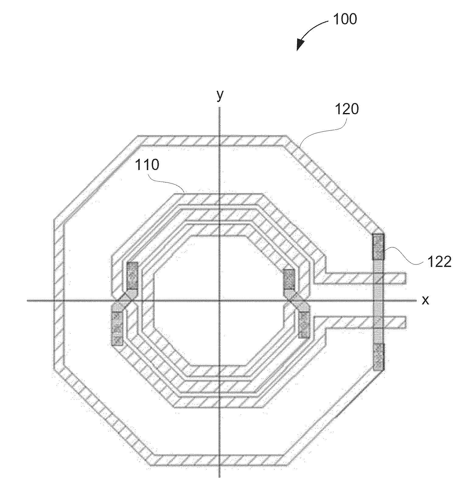
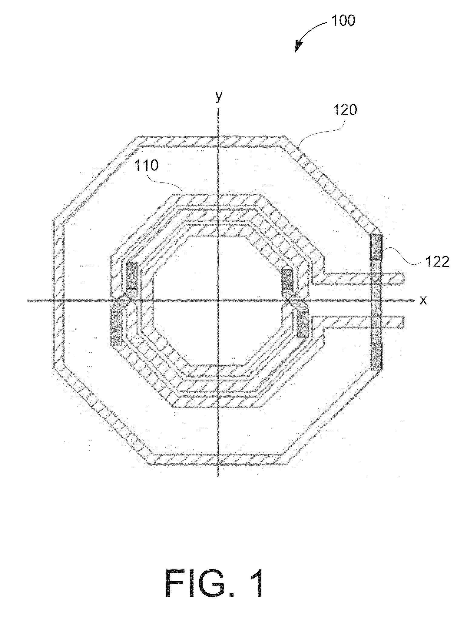
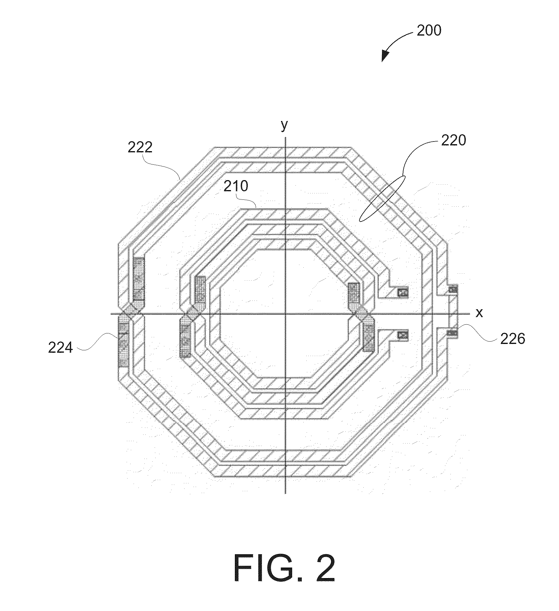
[0019]The present embodiments are described below in the context of on-chip inductors for simplicity only. It is to be understood that the present embodiments are equally applicable to magnetically shielding inductors made from discrete, integrated, and / or printed circuit components. In addition, the present shielding embodiments are not limited to inductors, but can be applied to any type of circuitry having inductive properties (e.g., transformers). As used herein, the term “inductor” may refer to inductive elements formed by a wire, a coil, a winding, and / or conductive traces formed on a silicon chip. Thus, the terms “inductor,”“coil,” and “winding” may be used interchangeably herein. Further, as used herein, the term “magnetic coupling” refers to the relationship between two circuit elements (e.g., inductors) wherein current changes in one element induces (e.g., through mutual inductance) a voltage and / or current in the other element.

[0020]In the following description, numerous ...


PUM

PropertyMeasurementUnit
magneticaaaaaaaaaa
distanceaaaaaaaaaa
circumferenceaaaaaaaaaa

Abstract

A magnetic shield for an inductor is disclosed that may substantially reduce unwanted magnetic coupling from other inductive circuitry. An inductive apparatus includes an inductor and a magnetic shield to shield the inductor from magnetic coupling effects. The magnetic shield includes an inductive ring formed from a plurality of turns surrounding the inductor. The magnetic shield may be used to reduce a magnetic coupling between the inductor and an inductive circuit element. Thus, the number of turns of the inductive ring may be based on the magnetic coupling between the inductor and the inductive circuit element. Further, a distance between the magnetic shield and the inductor may be based on the number of turns of the inductive ring. The distance between the magnetic shield and the inductor is to offset a magnetic coupling between the inductor and the magnetic shield.

Description

TECHNICAL FIELD[0001]The present embodiments relate generally to inductive circuits, and specifically to magnetic shields for reducing magnetic coupling between on-chip inductors.BACKGROUND OF RELATED ART[0002]Inductors and transformers are used in a wide variety of integrated circuit applications including radio frequency (RF) integrated circuit applications. An on-chip inductor is a passive electrical component that can store energy in a magnetic field created by the current passing through it. An inductor can be a conductor shaped as a coil which includes one or more “turns.” The turns concentrate the magnetic field flux induced by current flowing through each turn of the conductor in an “inductive” area within the inductor turns. The number of turns and the size of the turns affect the inductance.[0003]On-chip inductors are typically formed as helical or spiral traces in conductive layers (e.g., to form inductor turns). However, due to limitations in chip size, the performance o...

Claims


Application Information

Patent Timeline
Patent Type & Authority Applications(United States)
IPC IPC(8): H01F27/28H01F41/00
CPCH01F41/00H01F27/2885H01L23/5225H01L23/5227H01L2924/0002H01L2924/00
Inventor CHANG, RICHARD TZEWEIKAVOUSIAN, AMIRPOUYA
Owner QUALCOMM INC
Why Eureka
Try Eureka