Liquid crystal device and electronic apparatus

a liquid crystal device and electronic equipment technology, applied in the field of display devices, can solve the problems of inability to ensure a good sensitivity in the detection of pointing objects, and inability to achieve a good sensitivity in the detection of objects, so as to reduce unwanted irradiation of light, reduce the effect of undesirable irradiation

Inactive Publication Date: 2008-12-04
138 EAST LCD ADVANCEMENTS LTD
View PDF4 Cites 25 Cited by
  • Summary
  • Abstract
  • Description
  • Claims
  • Application Information

AI Technical Summary

Benefits of technology

[0016]In the configuration of a liquid crystal device according to the first aspect of the invention described above, it is preferable that the upper electrode should be formed in the same layer as that of the common electrode.
[0017]With such a preferred configuration, it is possible to form the upper electrode of the light-sensitive pickup element in an easier manner in comparison with a case where the upper electrode thereof is formed in the same layer as that of the pixel electrode.
[0018]In the configuration of a liquid crystal device according to the first aspect of the invention described above, it is preferable that the light-sensitive pickup element should have a lower electrode that is formed in the same layer as that of an electro-conductive layer that is electrically connected to a pixel-switching element.
[0019]The liquid crystal device having a preferred configuration described above offers a more (i.e., further) simplified and thus efficient production process because it is possible to manufacture the lower electrode

Problems solved by technology

A touch-panel-type liquid crystal device of the related art has a disadvantage in that, since it has a complex lamination/layer structure that is formed on the TFT array substrate thereof, it is not practically possible, or at best difficult, to secure a sufficient amount of light that reaches each of optical sensors thereof.
Therefore, as a disadvantage of the touch-panel-type liquid crystal device of the related art, it is not possible to ensure a good sensitivity in the detection of a pointing object that is performed by the optical sensors thereof.
In addition to such a disadvantage, if electrodes for optical sensors are form

Method used


Image

  • Liquid crystal device and electronic apparatus
  • Liquid crystal device and electronic apparatus
  • Liquid crystal device and electronic apparatus

Examples


first embodiment

1: First Embodiment

1-1: General Configuration of Liquid Crystal Device

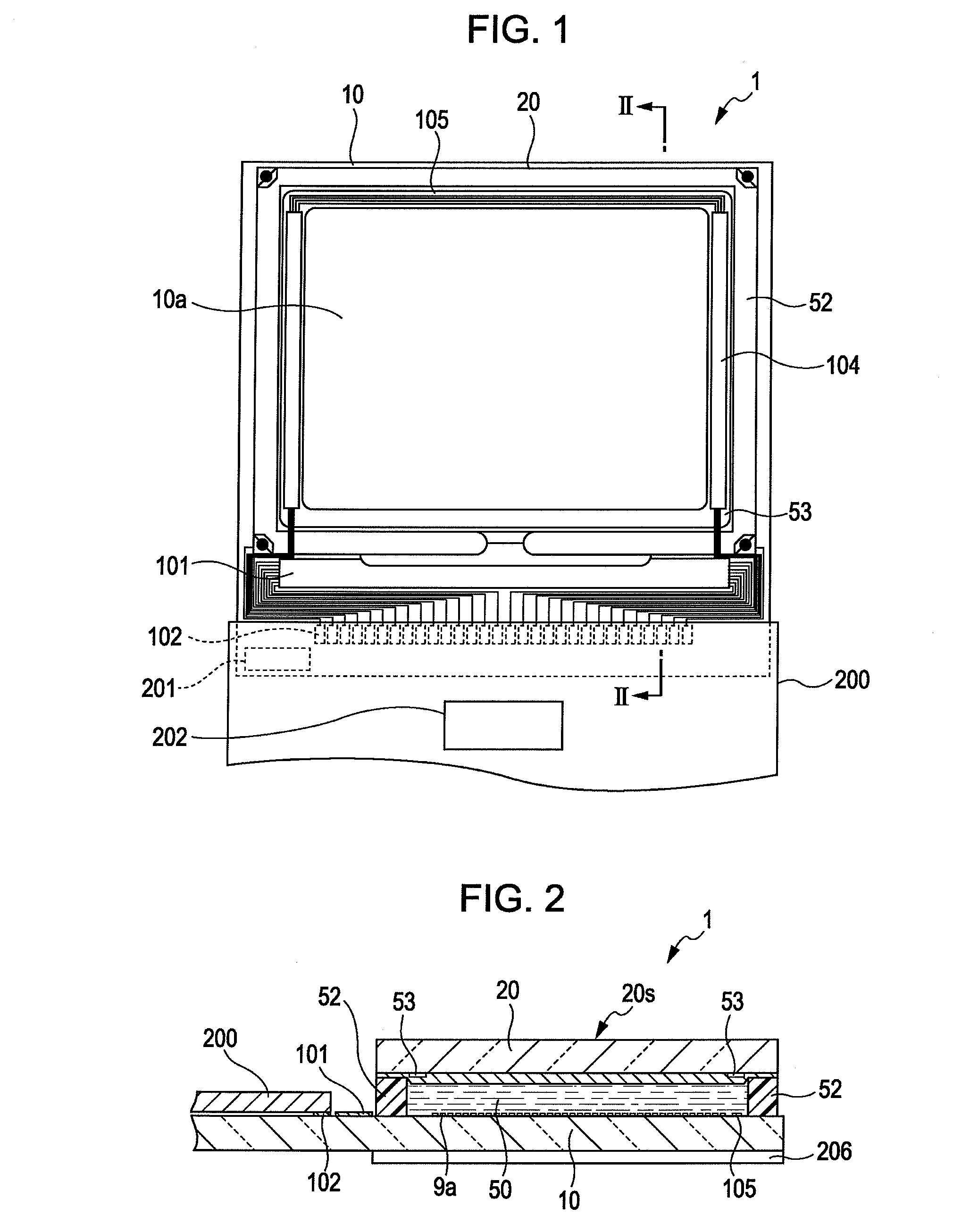
[0041]As illustrated in FIGS. 1 and 2, in the configuration of a liquid crystal device 1 according to the present embodiment of the invention, a TFT array substrate 10 and a counter substrate 20 are provided in such a manner that they face each other, that is, at positions opposite each other. The TFT array substrate 10 is a non-limiting example of a “first substrate” according to the invention, whereas the counter substrate 20 is a non-limiting example of a “second substrate” according to the invention. A liquid crystal layer 50 is sealed between the TFT array substrate 10 and the counter substrate 20. The TFT array substrate 10 and the counter substrate 20 are adhered to (e.g., bonded to) each other with the use of a sealant material 52 that is provided at a sealing region around an image display region 10a. The image display region 10a is a display area in which a plurality of pixel units (i.e., a plurality of ...

second embodiment

2: Second Embodiment

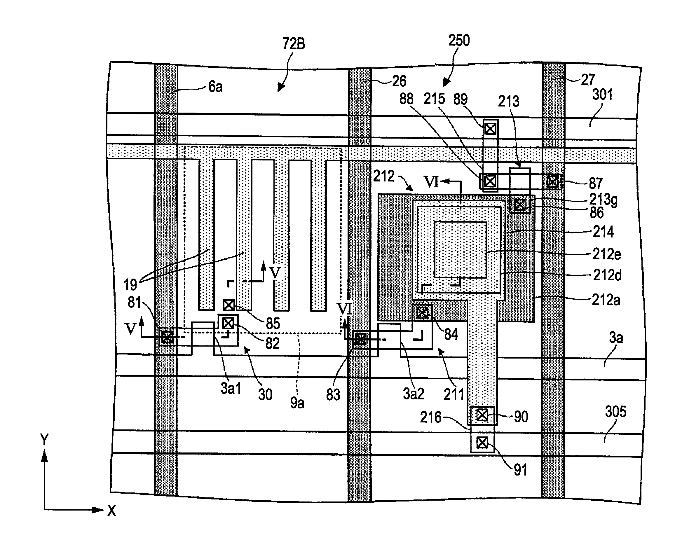
[0078]Next, with reference to FIGS. 7-9, a liquid crystal device according to a second embodiment of the invention is explained below. FIG. 7 is a plan view that schematically illustrates an example of the configuration of the sub pixel unit 72B-1 and the optical sensor unit 250 of a liquid crystal device according to a second embodiment of the invention. FIG. 8 is a sectional view taken along the line VIII-VIII of FIG. 7. FIG. 9 is a sectional view taken along the line IX-IX of FIG. 7. In the following description, the same reference numerals are assigned to the same components as those of the liquid crystal device 1 according to the first embodiment of the invention described above, and detailed explanation thereof is omitted.

[0079]As illustrated in FIG. 7, the sub pixel unit 72B-1 has the pixel electrode 9b. The pixel electrode 9b of the sub pixel unit 72B-1 is electrically connected to the TFT 30 thereof via two contact holes, that is, the contact hole 81 and...

third embodiment

3: Third Embodiment

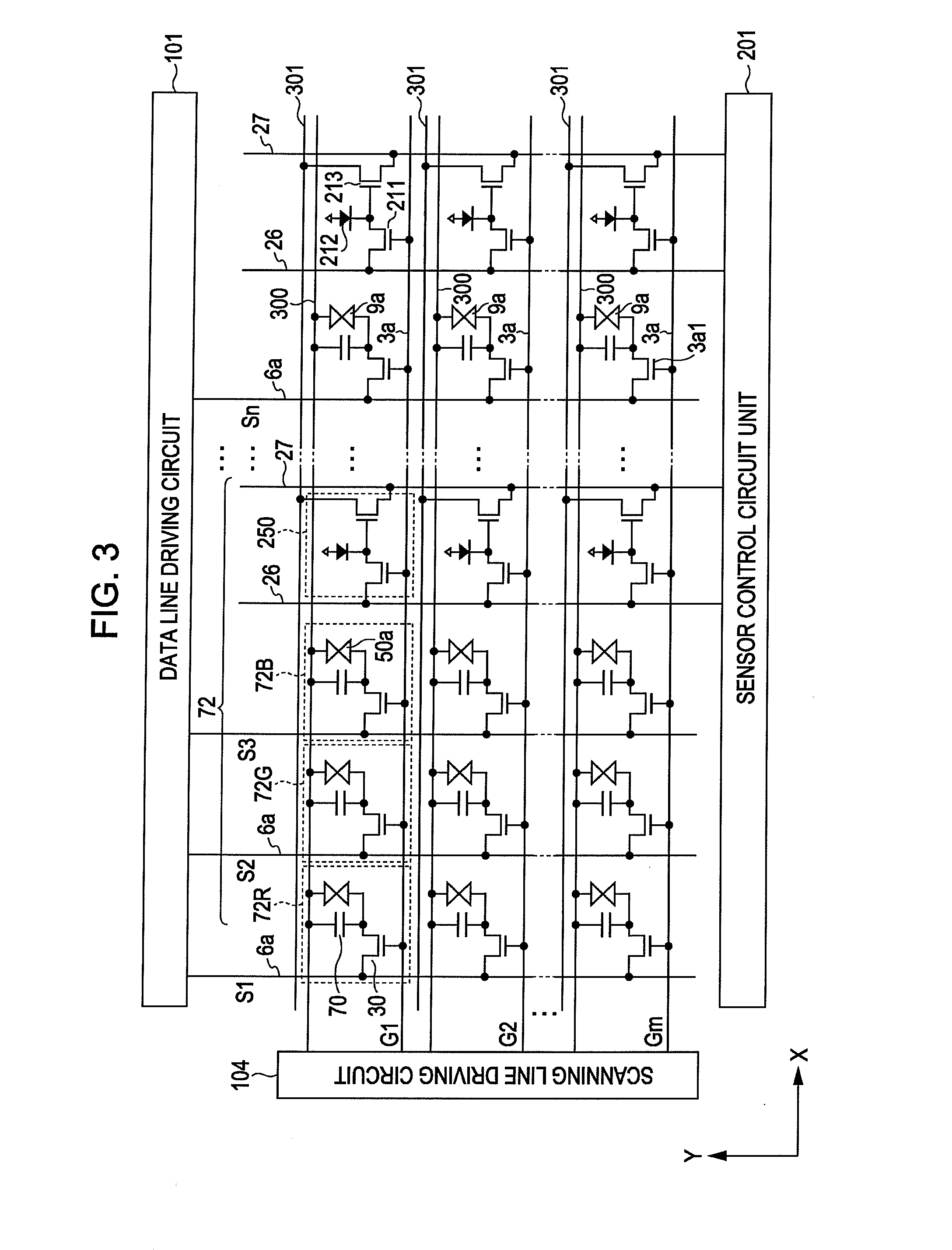
[0083]Next, with reference to FIGS. 10-12, a liquid crystal device according to a third embodiment of the invention is explained below. FIG. 10 is an equivalent circuit diagram that illustrates an example of constituent elements and wirings in a plurality of pixels that are arranged in a matrix pattern so as to constitute the image display region 10a of a liquid crystal device according to the present embodiment of the invention. FIG. 11 is a plan view that schematically illustrates an example of the configuration of the sub pixel unit 72B-2 and the optical sensor unit 250 of a liquid crystal device according to a third embodiment of the invention. FIG. 12 is a sectional view taken along the line XII-XII of FIG. 11.

[0084]The liquid crystal device according to the third embodiment of the invention illustrated in FIG. 10 differs from the above-described liquid crystal device according to the first or second embodiment of the invention in that one electrode of the PI...


PUM


Abstract

The invention provides a liquid crystal device that includes: a first substrate; a second substrate that is provided over the first substrate in such a manner that the first substrate and the second substrate face each other; a transparent pixel electrode that is provided in each of a plurality of pixels that constitute a display area over the first substrate; a transparent common electrode that is formed over the first substrate; a liquid crystal layer that is sandwiched between the first substrate and the second substrate, the liquid crystal layer containing liquid crystal molecules that are driven by a horizontal electric field that is generated in accordance with a difference between the electric potential of the pixel electrode and the electric potential of the common electrode; and a light-sensitive pickup element that is formed in the display area over the first substrate, the light-sensitive pickup element having an upper electrode that is formed in the same layer as that of either the pixel electrode or the common electrode.

Description

BACKGROUND[0001]1. Technical Field[0002]The present invention relates to a display device having an input sensing function such as a touch-panel-type liquid crystal device. In addition, the invention further relates to an electronic apparatus that is provided with such a display device.[0003]2. Related Art[0004]In the technical field to which the present invention pertains, a variety of display devices having a so-called touch panel input function has been proposed so far. In the configuration of a touch-panel-type liquid crystal device, which is an example of such a display device having a touch panel input function, an optical sensor (i.e., light sensor, photo sensor) is provided for either each of a plurality of pixel units or each of a plurality of groups of pixel units, where each group thereof is made up of a given number of pixel units. With such a configuration, in addition to its basic function of displaying an image by using light that transmits through the pixel units, a ...

Claims


Application Information

Patent Timeline
IPC IPC(8): G02F1/1343
CPCG02F1/13338G02F1/134363
Inventor EGUCHI, TSUKASA
Owner 138 EAST LCD ADVANCEMENTS LTD
Why Eureka
Try Eureka