Display substrate, manufacturing method thereof and flexible display device
a flexible display device and substrate technology, applied in the field of display substrates, can solve the problems of affecting the reliability affecting the performance of the tft, and a variety of vulnerable members on the flexible base substrate of the flexible display device are liable to be damaged, so as to improve the reliability of the display substra
- Summary
- Abstract
- Description
- Claims
- Application Information
AI Technical Summary
Benefits of technology
Problems solved by technology
Method used
Image
Examples
embodiment 1
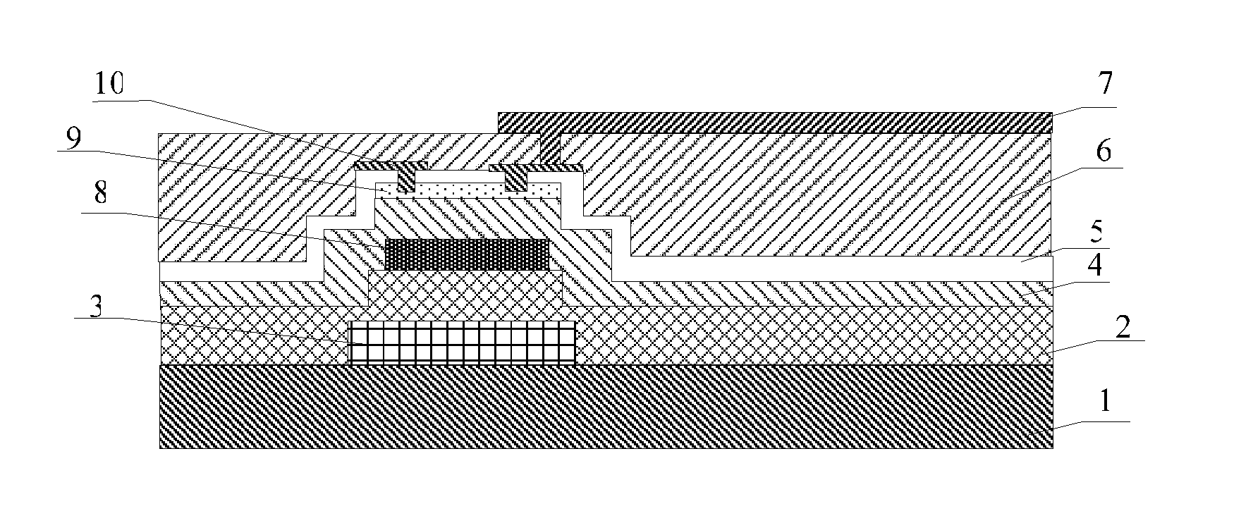
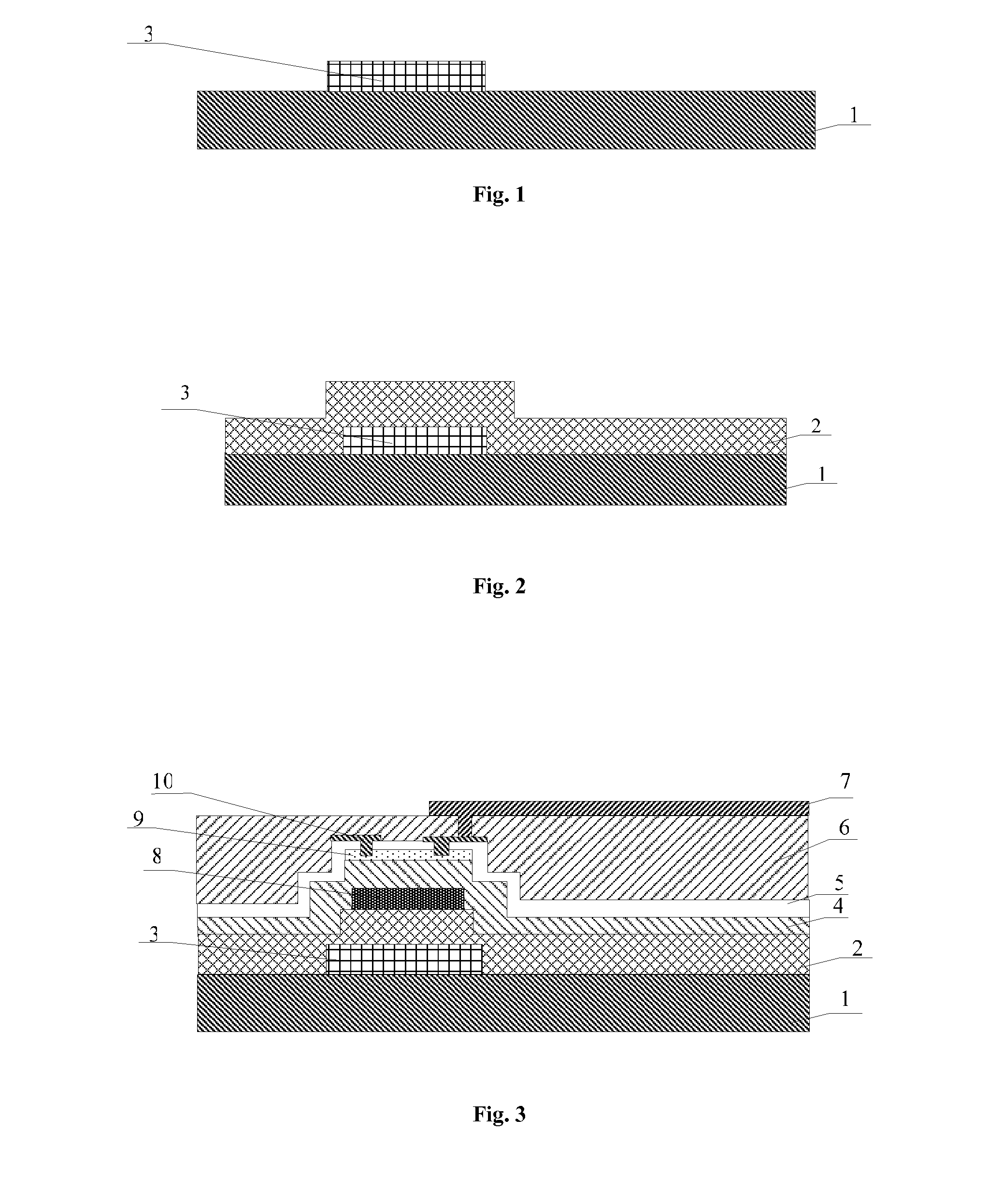
[0039]As shown in FIG. 1 to FIG. 3, this embodiment provides a display substrate, including a polyimide (PI) base substrate 1 and a TFT (used as an example of a vulnerable member) arranged on the PI base substrate, wherein a stress absorption layer 3 is arranged between the PI base substrate 1 and the TFT; the stress absorption layer 3 is formed by a patterning process, for example, the stress absorption layer 3 is formed by performing a patterning process by adopting a mask plate corresponding to the shape of the TFT.
[0040]As shown in FIG. 3, the projection of the TFT on the PI base substrate 1 is within the projection region of the stress absorption layer 3 on the PI base substrate 1. Preferably, the projection of the TFT on the base substrate coincides with the projection of the stress absorption layer 3 on the base substrate, namely, the stress absorption layer 3 is only arranged below the TFT. Therefore, stress generated when the display substrate is bent may be dispersed throu...
embodiment 2
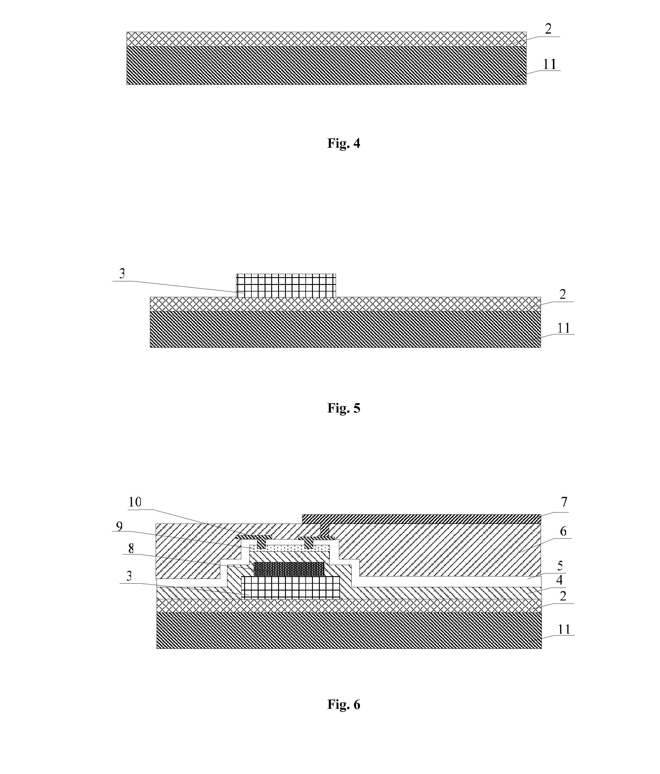
[0057]As shown in FIG. 4 to FIG. 6, this embodiment provides a display substrate, including a polyethylene glycol terephthalate (PET) base substrate 11 and a TFT (used as an example of a vulnerable member) arranged on the PET base substrate 11, wherein a stress absorption layer 3 is arranged between the PET base substrate 11 and the TFT; the stress absorption layer 3 is formed by a patterning process, for example, the stress absorption layer 3 is formed by performing a patterning process by adopting a mask plate corresponding to the shape of the TFT (used as the example of the vulnerable member).
[0058]As shown in FIG. 6, the projection of the TFT on the PET base substrate 11 is within the projection region of the stress absorption layer 3 on the PET base substrate 11. Preferably, the projection of the TFT on the base substrate coincides with the projection of the stress absorption layer 3 on the base substrate. The stress absorption layer 3 is not arranged on part of the PI base sub...
embodiment 3
[0075]This embodiment provides a flexible display device, including the above-mentioned display substrate and other necessary assemblies. Preferably, the display substrate included in the flexible display device is a flexible organic light emitting diode display substrate.
PUM
 Abstract
Description
Claims
Application Information
 - R&D
- Intellectual Property
- Life Sciences
- Materials
- Tech Scout
- Unparalleled Data Quality
- Higher Quality Content
- 60% Fewer Hallucinations
Browse by: Latest US Patents, China's latest patents, Technical Efficacy Thesaurus, Application Domain, Technology Topic, Popular Technical Reports.
© 2025 PatSnap. All rights reserved.Legal|Privacy policy|Modern Slavery Act Transparency Statement|Sitemap|About US| Contact US: help@patsnap.com


