

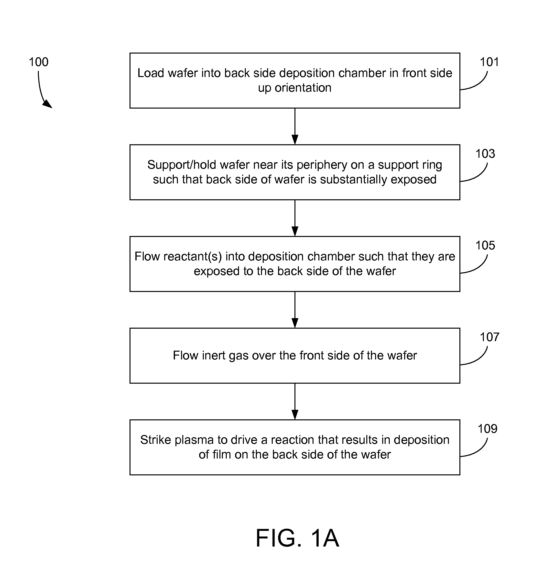
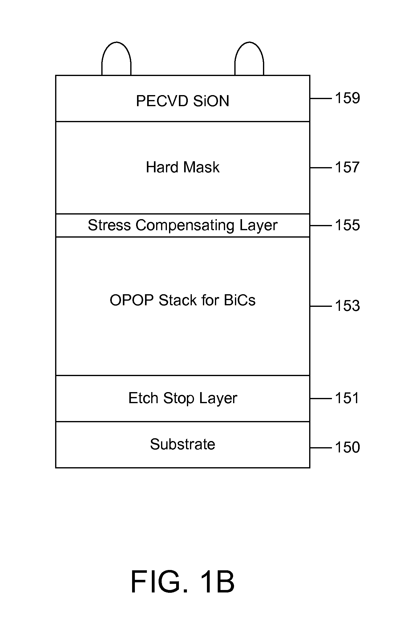
Back side deposition apparatus and applications
- Summary
- Abstract
- Description
- Claims
- Application Information
AI Technical Summary
Benefits of technology
Problems solved by technology
Method used
Image

Examples
Embodiment Construction
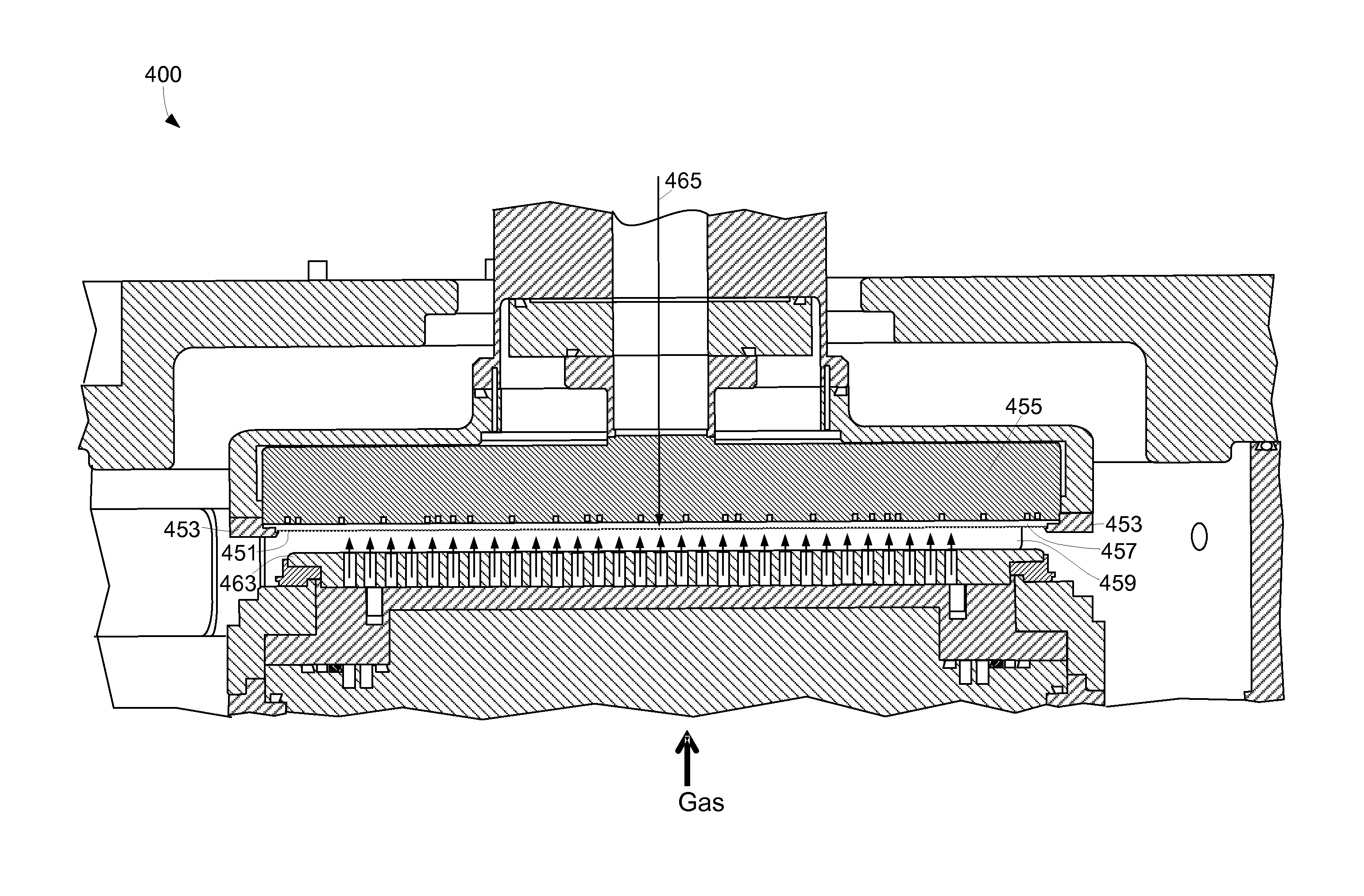
[0026]In this application, the terms “semiconductor wafer,”“wafer,”“substrate,”“wafer substrate,” and “partially fabricated integrated circuit” are used interchangeably. One of ordinary skill in the art would understand that the term “partially fabricated integrated circuit” can refer to a silicon wafer during any of many stages of integrated circuit fabrication thereon. A wafer or substrate used in the semiconductor device industry typically has a diameter of 200 or 300 mm, though the industry is moving toward adoption of 450 mm diameter substrates. The description herein uses the terms “front” and “back” to describe the different sides of a wafer substrate. It is understood that the front side is where most deposition and processing occurs, and where the semiconductor devices themselves are fabricated. The back side is the opposite side of the wafer, which typically experiences minimal or no processing during fabrication.
[0027]The flow rates and power levels provided herein are ap...
PUM
| Property | Measurement | Unit |
|---|---|---|
| Thickness | aaaaa | aaaaa |
| Height | aaaaa | aaaaa |
| Height | aaaaa | aaaaa |
Abstract
Description
Claims
Application Information