Nitride semiconductor element and method for manufacturing the same

Active Publication Date: 2015-12-03
NICHIA CORP
View PDF1 Cites 4 Cited by
  • Summary
  • Abstract
  • Description
  • Claims
  • Application Information

AI Technical Summary

Benefits of technology

[0010]According to embodiments of the present invention, the nitride semiconductor element includes a nitride semiconductor layer having a low dislocation density and grown from the sapphire substrate with the elongated projections, and thus can have improved temperature characteristics. Further, according to embodiments of the

Problems solved by technology

However, if timing of crystal growth differs between the bottom surface of the trench and an uppe

Method used


Image

  • Nitride semiconductor element and method for manufacturing the same
  • Nitride semiconductor element and method for manufacturing the same
  • Nitride semiconductor element and method for manufacturing the same

Examples


Example

First Embodiment

Structure of Nitride Semiconductor Element

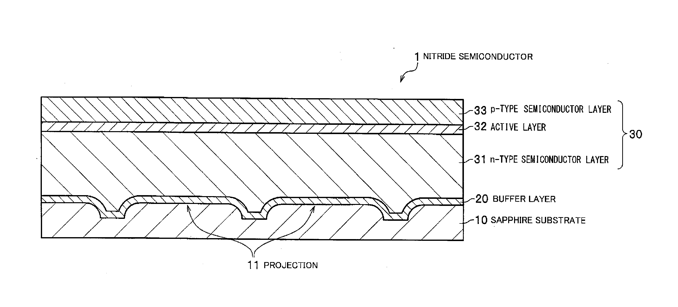
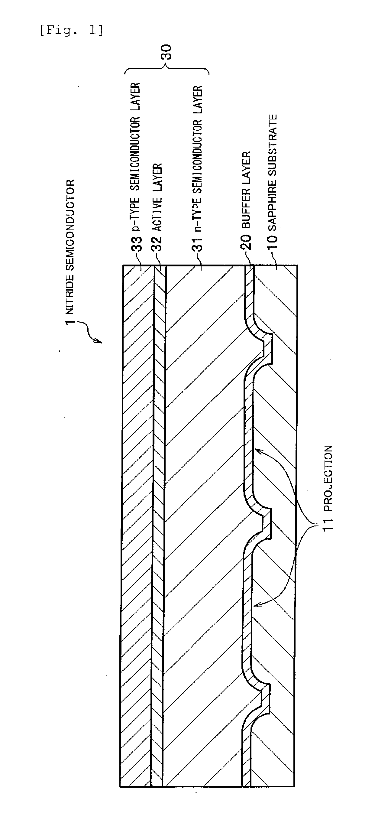
[0026]The structure of a nitride semiconductor element according to a first embodiment of the present invention will be described below with reference to FIGS. 1 to 4. As shown in FIG. 1, a nitride semiconductor element 1 has a stacked structure, in which a sapphire substrate 10 serving as a substrate for nitride semiconductor element, a buffer layer 20 and a nitride semiconductor layer 30 are stacked.

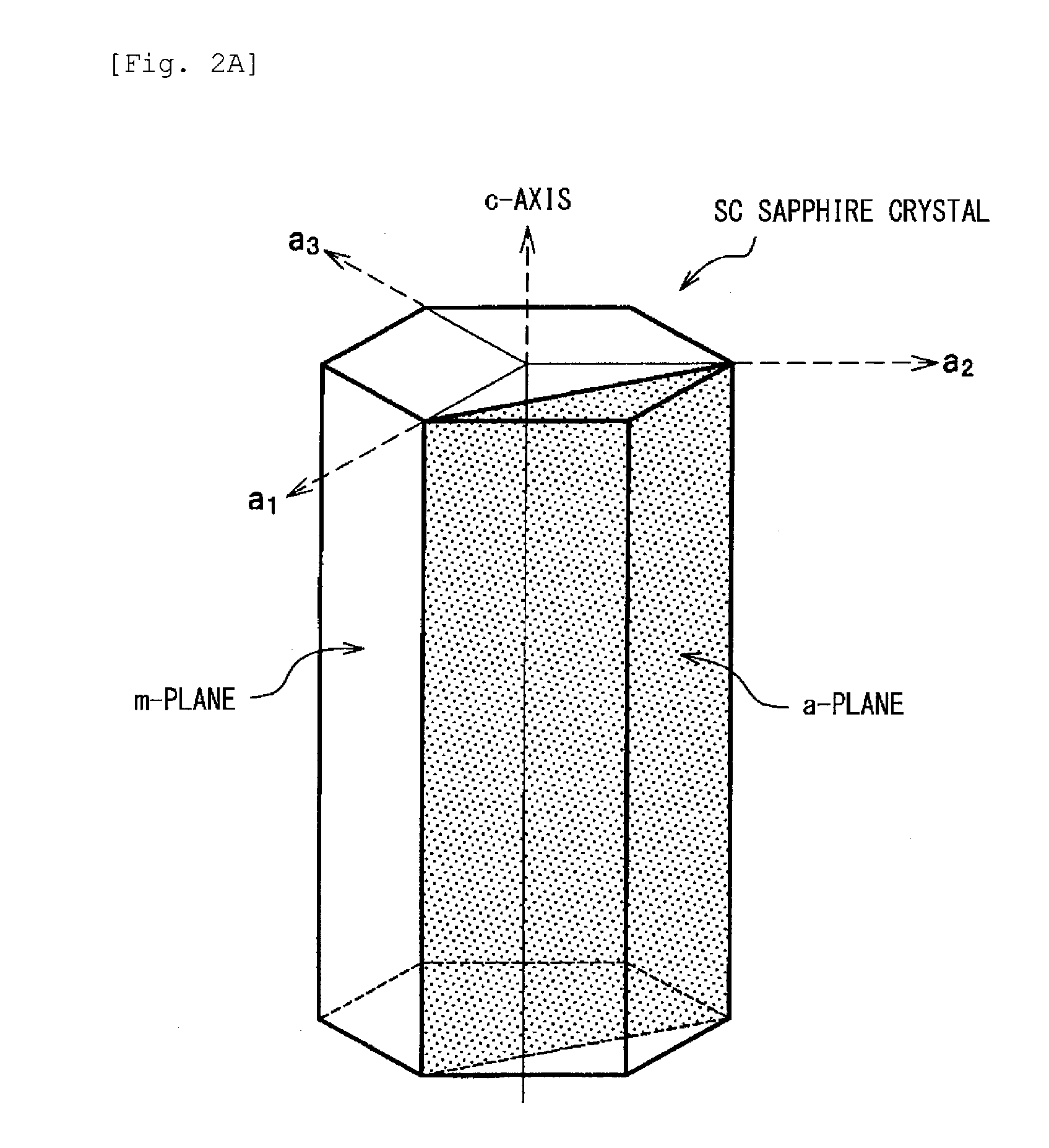
[0027]The sapphire substrate (substrate for nitride semiconductor element) 10 is to grow a nitride semiconductor (e.g., GaN) thereon, while supporting the nitride semiconductor layer 30. As shown in FIGS. 1 and 3, the sapphire substrate 10 is formed in a flat plate shape, and has on its upper surface, a plurality of projections 11 (convex portion 11) formed in an elongated shape in a plan view. The sapphire substrate 10 including the above-mentioned projections 11 is formed in a thickness of, e.g., 50 μm to 300 μm as a whole.

[00...

Example

Second Embodiment

[0062]As illustrated in the plan view of FIG. 10, the projections 11 of a nitride semiconductor element according to a second embodiment are arranged at the surface on the c-plane side of a sapphire substrate 10A in the longitudinal direction (in the right-left direction of FIG. 10) of the projections 11 as well as in the width direction (in the up-down direction of FIG. 10) at respective predetermined intervals. Specifically, as illustrated in FIG. 10, the projections 11 are arranged at the respective predetermined intervals in the row direction, which is the longitudinal direction of the elongated shape, as well as in the column direction, which is the width direction of the elongated shape. Further, the projections 11 belonging to the rows adjacent to each other in the column direction may be arranged to be located in the same position in the row direction, and the projections 11 belonging to the columns adjacent to each other in the row direction may be arranged...

Example

Third Embodiment

[0065]As illustrated in the plan view of FIG. 11, in a nitride semiconductor element according to a third embodiment, the projections 11 are arranged at the surface on the c-plane side of a sapphire substrate 10B at respective predetermined intervals in directions having different angles while the outer edges in the longitudinal direction of the projections 11 faces each other. Specifically, the projections 11 include a first group of projections (a first group) 11A, in which each of outer edges in the longitudinal direction of the elongated shape of the projections 11 extends in the first direction, and a second group of projections (a second group) 11B, in which each of outer edges in the longitudinal direction of the elongated shape of the projections 11 extends in a second or third direction (the nitride semiconductor element of the third embodiment may include the first group of projections 11A and the second group of projections 11B).

[0066]Here, the first, seco...


PUM


Abstract

A nitride semiconductor element includes a sapphire substrate including: a main surface extending in a c-plane of the sapphire substrate, and a plurality of projections disposed at the main surface, the plurality of projections including at least one projection having an elongated shape in a plan view; and a nitride semiconductor layer disposed on the main surface of the sapphire substrate. The at least one projection has an outer edge extending in a longitudinal direction of the elongated shape, the outer edge extending in a direction oriented at an angle in a range of −10° to +10° with respect to an a-plane of the sapphire substrate in the plan view.

Description

CROSS-REFERENCE TO RELATED APPLICATIONS[0001]The present application claims priority on Japanese Patent Application No. 2014-111966, filed May 30, 2014, and Japanese Patent Application No. 2015-107307, filed May 27, 2015, which are incorporated by reference in their entireties.BACKGROUND[0002]1. Technical Field[0003]The present disclosure relates to a nitride semiconductor element that is formed by crystal growth from a substrate, and a method for manufacturing the same.[0004]2. Description of the Related Art[0005]A light emitting diode (LED) made of a nitride semiconductor is normally formed by sequentially stacking an n-type semiconductor layer, an active layer and a p-type semiconductor layer on a sapphire substrate. Conventionally, there has been proposed a technique which involves providing a structure with elongated recess portions or a composite structure with elongated projection and recess portions at a sapphire substrate in advance in order to improve the light emission ef...

Claims


Application Information

Patent Timeline
IPC IPC(8): H01L33/22H01L33/32H01L33/12H01L33/00H01L33/06
CPCH01L33/22H01L33/0025H01L33/0066H01L33/32H01L33/06H01L33/12H01L33/0075H01L33/007H01L33/025H01L33/16H01L33/20
Inventor SHIMOOKA, TOMOHIROSANO, MASAHIKOAZUMA, NAOKI
Owner NICHIA CORP
Why Eureka
Try Eureka