Optically guided microdevice comprising a nanowire

a nanowire and optical guide technology, applied in nanotechnology, scanning probe microscopy, instruments, etc., can solve the problems of being able to radiate light to and from the nanowire, and achieve the effect of improving inspection of objects, facilitating the use, and facilitating a new area of micro or nano-endoscopic applications rendering

Inactive Publication Date: 2015-12-10
DANMARKS TEKNISKE UNIV
View PDF4 Cites 16 Cited by
  • Summary
  • Abstract
  • Description
  • Claims
  • Application Information

AI Technical Summary

Benefits of technology

[0045]The nanowire may in an advantageous embodiment further be optically arranged for receiving electromagnetic radiation from an associated object and transmit it to the first electromagnetic radiation emitting unit, this unit also being arranged for transmitting the said electromagnetic radiation out of the microdevice, the microdevice thereby functioning as a bi-directional optically device. This facilitates the use of the microdevice as an optical probe being optically displaceable. The microdevice with the nanowire may be considered as a moveable extension or ‘local lens’ of e.g. optical equipment applied for optical imaging or analysis.
[0046]Preferably, the nanowire may be manufactured in a biofriendly material suitable for endoscopic application, such as SnO2, and graphene. In fact, the present invention facilitates a new area of micro- or nano-endoscopic applications rendering e.g. intra-cellular endoscopic analysis feasible as explained in more detail above.
[0047]The electromagnetic radiation in-coupling element may be arranged to receive incoming electromagnetic radiation having a first direction and the electromagnetic radiation out-coupling element may be arranged to emit electromagnetic radiation having a second direction where the first direction and the second direction are non-parallel, alternatively the first direction and the second direction are parallel but displaced, more alternatively where the first direction and the second direction are anti-parallel. This is advantageous in order to provide improved inspection of objects having complex shapes and / or sizes, which makes a turned direction of inspection desirable.

Problems solved by technology

However, it may be problematic to be able to radiate light to and from the nanowire, particularly because the nanowire is not freely moveable, both with respect to translation and rotation, relative to the controlling beams of radiation.

Method used


Image

  • Optically guided microdevice comprising a nanowire
  • Optically guided microdevice comprising a nanowire
  • Optically guided microdevice comprising a nanowire

Examples


Embodiment Construction

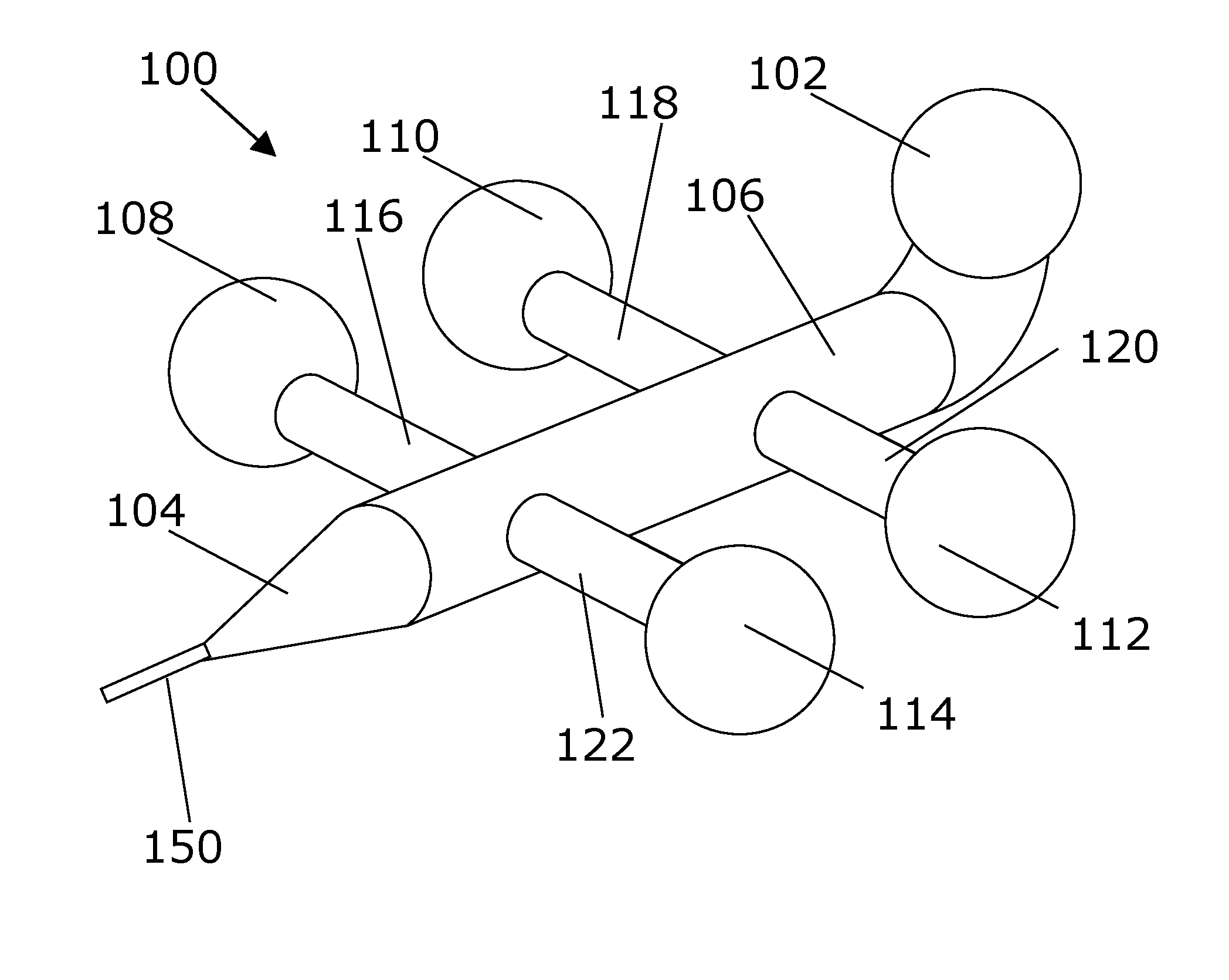
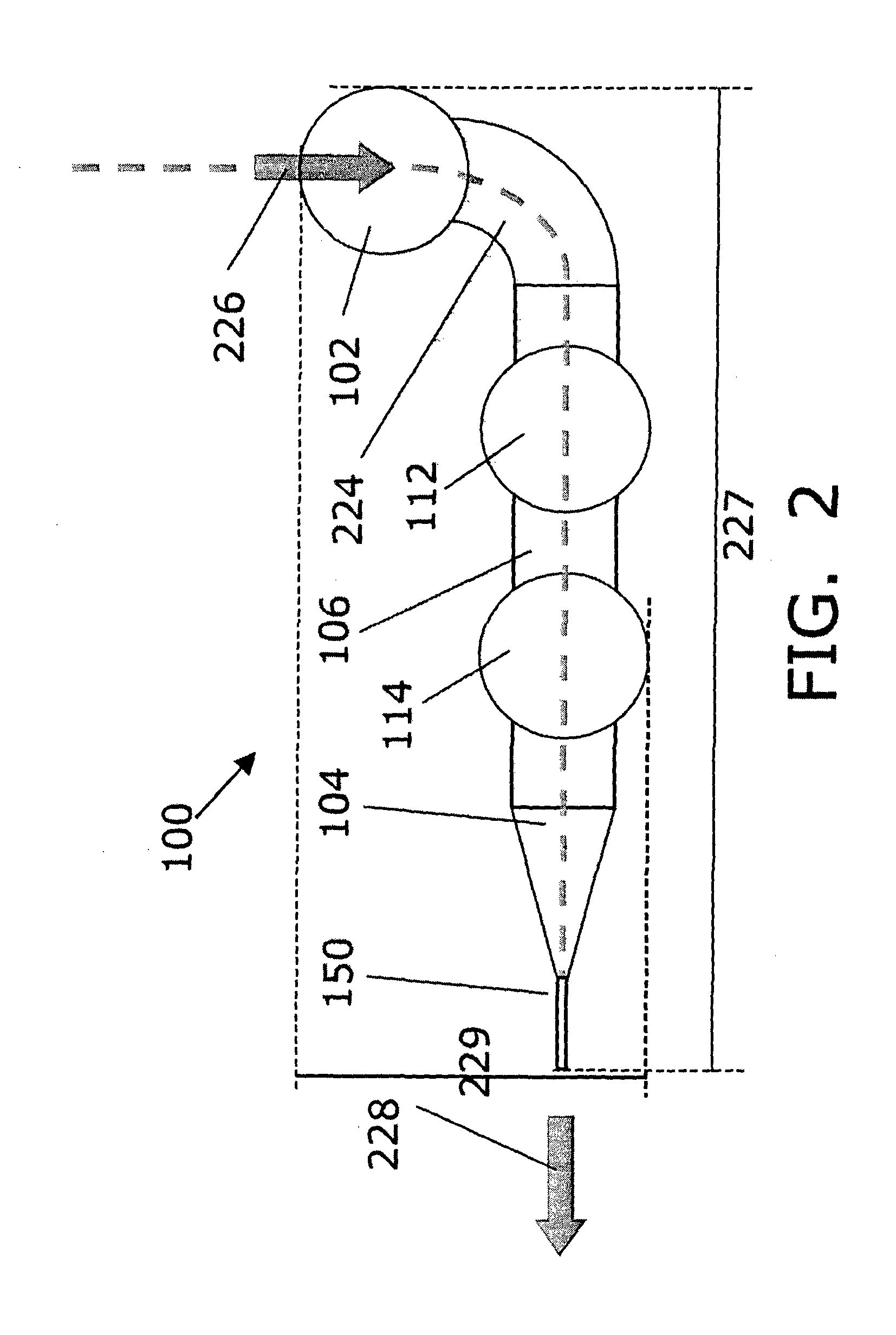
[0093]In the following section, light is used interchangeably with EMR. It is understood that light may be used in particular embodiments, but that the exemplary use of light in those embodiments do not constrain the invention to use of light only. FIG. 1 shows a perspective view of a microdevice 100 according to an embodiment of the invention, the microdevice 100 features a light in-coupling element 102, a light out-coupling element 104, and nanowire 150 being arranged for receiving electromagnetic radiation emitted from the first electromagnetic radiation emitting unit 102 and emitting electromagnetic radiation through the microdevice body towards the nanowire 150. The relative size of the nanowire with respect to the microdevice is not to scale. The light in-coupling element 102 is arranged to receive light and guide the received light into a light guiding element 106 which optically connects the light in-coupling element with the light out-coupling element. Thus, light may be re...


PUM


Abstract

The present invention relates to a microdevice (100) for emitting electromagnetic radiation onto an associated object. Simultaneous non-contact spatial control over the microdevice in terms of translational movement in three dimensions, and rotational movement around at least two axes, preferably three axes, is possible. The microdevice further comprises a nanowire (150) being arranged for emitting electromagnetic radiation onto said associated object. This is advantageous for obtaining better spatial control of the microdevice comprising the nanowire, and this enables that light could more effectively be coupled into the nanowire. This opens up for a much wider application of nanowires in optics because of the improved spatial control.

Description

FIELD OF THE INVENTION[0001]The present invention relates to a microdevice for investigating or analyzing an associated object, and more specifically to a device and a method for facilitating investigating or analyzing an associated object with electromagnetic radiation.BACKGROUND OF THE INVENTION[0002]Within the field of investigation or analyzing objects with electromagnetic radiation it is of constant appeal to be able to improve the instruments used to gain information about the examined objects. For example, it is a desire to improve the spatial resolution. Another desire is to expand the types of objects which can be examined. The field has spawned a large number of techniques which each have contributed to the general progress of the field. Examples include confocal microscopy and scanning near field optical microscopy. Recently, the use of nanowires has attracted attention. Inorganic nanowires may have diameters substantially below the wavelength of visible light, and their ...

Claims


Application Information

Patent Timeline
Patent Type & Authority Applications(United States)
IPC IPC(8): G01Q60/22
CPCG01Q60/22Y10S977/954B82Y20/00B82Y15/00G01Q70/12G02B6/107G02B21/32G02B23/26
Inventor GLUCKSTAD, JESPER
Owner DANMARKS TEKNISKE UNIV
Why Eureka
Try Eureka