
Active matrix substrate, display device, defect modification method for display device, and method for manufacturing display device

a technology of active matrix substrate and defect modification method, which is applied in the direction of semiconductor devices, instruments, electrical devices, etc., can solve the problems of display defect, no longer properly supplied signals, and pixels cannot produce intended displays

Inactive Publication Date: 2015-12-10
SHARP KK
View PDF2 Cites 11 Cited by
  • Summary
  • Abstract
  • Description
  • Claims
  • Application Information

AI Technical Summary

Benefits of technology

The present invention provides an active matrix substrate that can repair display defects caused by wire breaks along bus lines. Additionally, a display device that utilizes this active matrix substrate is also provided.

Problems solved by technology

Signals are no longer properly supplied to TFTs of pixels located downstream of the wire break location, and those pixels can no longer produce an intended display.
Thus, a wire break along a bus line can lead to a display defect.

Method used


Image

  • Active matrix substrate, display device, defect modification method for display device, and method for manufacturing display device
  • Active matrix substrate, display device, defect modification method for display device, and method for manufacturing display device
  • Active matrix substrate, display device, defect modification method for display device, and method for manufacturing display device

Examples


embodiment 1

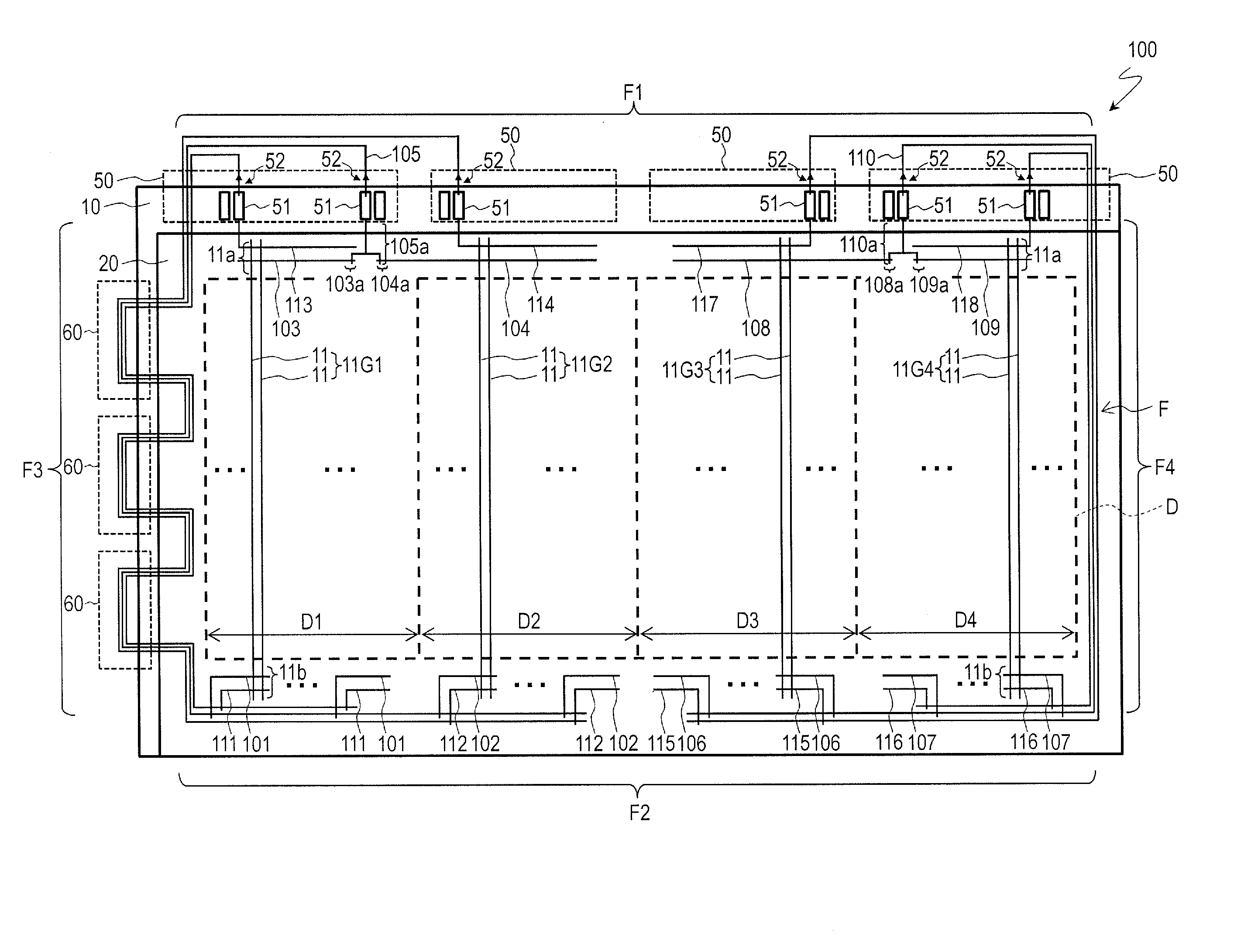
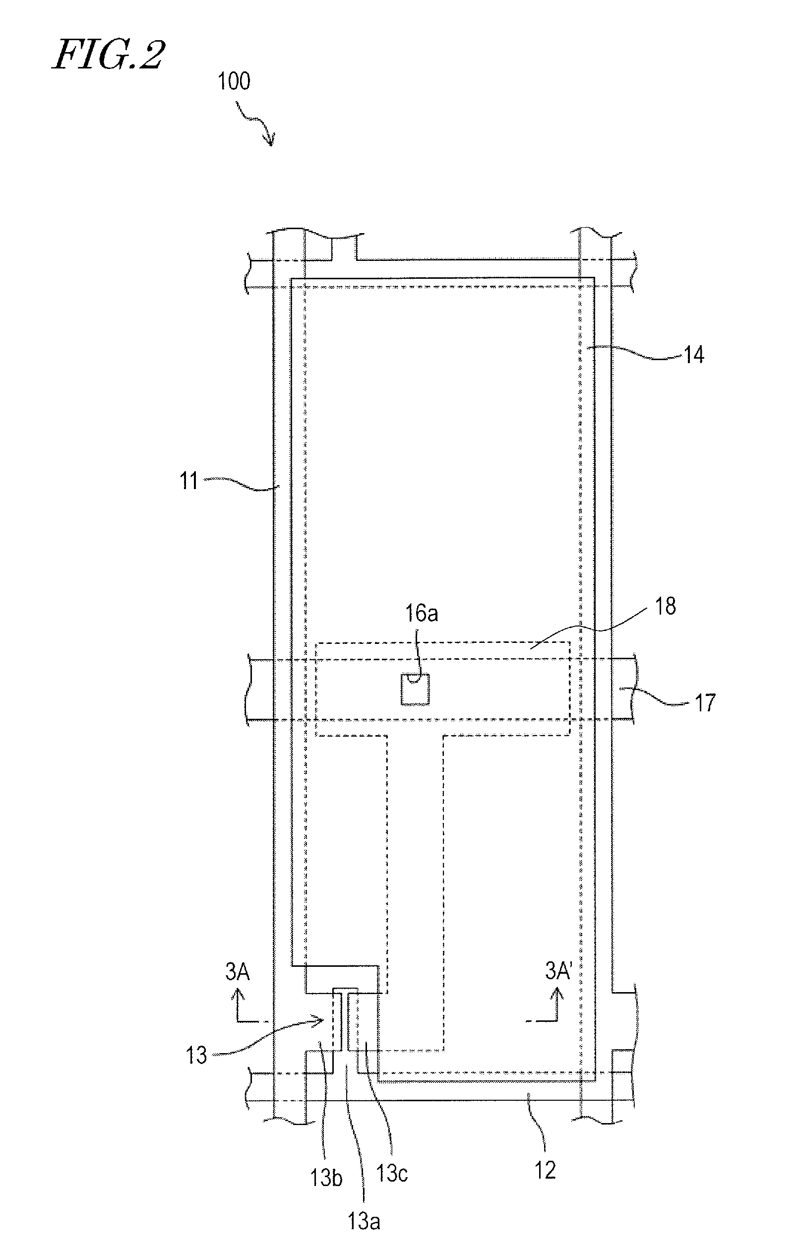
[0043]FIGS. 1, 2 and 3 show a liquid crystal display device 100 of the present embodiment. FIG. 1 is a plan view schematically showing the liquid crystal display device 100. FIG. 2 is a plan view schematically showing an area of the liquid crystal display device 100 corresponding to one pixel. FIG. 3 is a cross-sectional view taken along line 3A-3A′ of FIG. 2.

[0044]The liquid crystal display device 100 includes a display region D and a non-display region F, as shown in FIG. 1. The display region D is defined by a plurality of pixels arranged in a matrix pattern. The display region D is divided into a first, second, third and fourth block D1, D2, D3 and D4. The non-display region F is provided outside (around) the display region. The non-display region F is a bezel-shaped region including a first, second, third and fourth area F1, F2, F3 and F4, and is referred to also as the “bezel region”.

[0045]The liquid crystal display device 100 includes an active matrix substrate (hereinafter r...

embodiment 2

[0116]FIG. 11 shows a liquid crystal display device 200 of the present embodiment. FIG. 11 is a plan view schematically showing the liquid crystal display device 200. The following description will focus on how the liquid crystal display device 200 differs from the liquid crystal display device 100 of Embodiment 1.

[0117]The liquid crystal display device 200 of the present embodiment differs from the liquid crystal display device 100 of Embodiment 1 in that the eleventh to eighteenth repair lines 111 to 118 are absent, as shown in FIG. 11. By omitting the eleventh to eighteenth repair lines 111 to 118, it is possible to reduce the bezel width.

[0118]Note that the first to tenth repair lines 101 to 110 may be omitted instead of omitting the eleventh to eighteenth repair lines 111 to 118, but it is more preferable to omit the eleventh to eighteenth repair lines 111 to 118 as in the present embodiment. By keeping the first to tenth repair lines 101 to 110, there can be fewer external con...

embodiment 3

[0120]FIG. 12 shows the liquid crystal display device 300 of the present embodiment. FIG. 12 is a plan view schematically showing the liquid crystal display device 300. The following description will focus on how the liquid crystal display device 300 differs from the liquid crystal display device 200 of Embodiment 2.

[0121]The liquid crystal display device 300 of the present embodiment differs from the liquid crystal display device 200 of Embodiment 2 in that the fifth repair line 105 is routed so as not to run in the third area F3 of the non-display region F. The fifth repair line 105 of the liquid crystal display device 300 is routed so as to extend from the first area F1 to the second area F2 via the fourth area F4 of the non-display region F.

[0122]Although the fifth repair line 105 of the liquid crystal display device 200 of Embodiment 2 can be provided so that no portions thereof are formed on the second FPC 60 (i.e., so as not to run through the second FPC 60) in the third area...


PUM


Abstract

An active matrix substrate (10) includes a first line (101), a second line (102), a third line (103), a fourth line (104) and a fifth line (105) provided in a non-display region F. The first line crosses a non-input-side end portion of at least one bus line of a first bus line group with an insulating layer interposed therebetween. The second line crosses a non-input-side end portion of at least one bus line of a second bus line group with an insulating layer interposed therebetween. The third line crosses an input-side end portion of the first bus line group with an insulating layer interposed therebetween, and does not cross the second bus line group. The fourth line crosses an input-side end portion of the second bus line group with an insulating layer interposed therebetween, and does not cross the first bus line group. The fifth line is routed so as to cross the first, second, third and fourth lines with an insulating layer interposed therebetween. The third line and the fourth line are electrically separated from each other.

Description

TECHNICAL FIELD[0001]The present invention relates to an active matrix substrate. The present invention also relates to a display device, a method for repairing a defect of a display device, and a method for manufacturing a display device.BACKGROUND ART[0002]Liquid crystal display devices, which have small thicknesses and low power consumptions, have been used widely in various fields. Particularly, active matrix-type liquid crystal display devices including a thin film transistor (TFT) for each pixel, which have high specifications with high contrast ratios and desirable response characteristics, have been used in TVs, monitors, laptop computers, and the like, and have recently extended their market size.[0003]An active matrix-type liquid crystal display device includes an active matrix substrate having a plurality of TFTs formed thereon, and a color filter substrate provided so as to oppose the active matrix substrate, wherein the orientation of the liquid crystal layer sandwiched...

Claims


Application Information

Patent Timeline
Patent Type & Authority Applications(United States)
IPC IPC(8): H01L27/12
CPCH01L27/1244H01L27/1259H01L27/1225H01L27/1222G02F1/136259H01L27/124G02F1/136263
Inventor ITOH, RYOHKI
Owner SHARP KK
Learn More