Method for programming a bipolar resistive switching memory device

a memory device and bipolar resistive technology, applied in the direction of static storage, pulse generators, instruments, etc., can solve the problems of complex routing and switching circuits, bipolar programming memory devices, application of negatives

Active Publication Date: 2015-12-24
COMMISSARIAT A LENERGIE ATOMIQUE ET AUX ENERGIES ALTERNATIVES
View PDF28 Cites 21 Cited by
  • Summary
  • Abstract
  • Description
  • Claims
  • Application Information

AI Technical Summary

Benefits of technology

[0019]One purpose of this invention is also to propose an electronic circuit comprising at least one bipolar switching memory device, for which the programming of the memory device does not require the use of negative electric potentials or complex routing and switching circuits to carry a data signal from both sides of the memory device.
[0031]Given that the flow of current through the memory device is only allowed by the selection device during a programming time which is included in the time period d, the value of the data signal is therefore stable throughout the programming time of the memory device, thus guaranteeing good stability when programming the memory device. Furthermore, because the control signal applied to the second electrode of the memory device is the same when programming the memory device in a high-resistance state or low-resistance state, the management of the control signal is simplified compared to that of a control signal whose value must be adapted depending on the state in which a memory device must be programmed.
[0032]Moreover, because the control signal applied to the second electrode of the memory device is the same when programming the memory device in a high-resistance state or low-resistance state and because the change from state 0 to state 1, or from state 1 to state 0, of the control signal takes place during the programming time (time during which the value of the data signal does not change), a single value alternation of the control signal state suffices throughout the programming time to program the memory device in the desired state. This prevents the need to reset the device memory state before programming to the desired value, and therefore prevents an unnecessary aging of the memory device due to a systematic reset of the memory device state before each programming operation.
[0037]One of the first and second electrodes may be electrically linked to the source or to the drain of at least one first selection MOS transistor, and, during at least one part of the time period d, the selection MOS transistor may be in the ON state. The first selection MOS transistor may form part of the selection device and be intended to be in the ON state throughout the programming time. Aside from the selection role of the memory device, the state of which is intended to be programmed, such an MOS transistor is also used to limit the current flowing through the memory device during its programming, and therefore helps adapt this current to suit the nature of the memory device.

Problems solved by technology

Such bipolar programming memory devices therefore have the disadvantages of requiring the application of a negative voltage at the electrode terminals of the memory device, via the application of a negative electric potential on the active electrode, in order to programme one of the memory states (OFF state).
However, this requires the creation of complex routing and switching circuits, such as those described in documents US 2010 / 110765 A1 and US 2007 / 132049 A1.

Method used


Image

  • Method for programming a bipolar resistive switching memory device
  • Method for programming a bipolar resistive switching memory device
  • Method for programming a bipolar resistive switching memory device

Examples


first embodiment

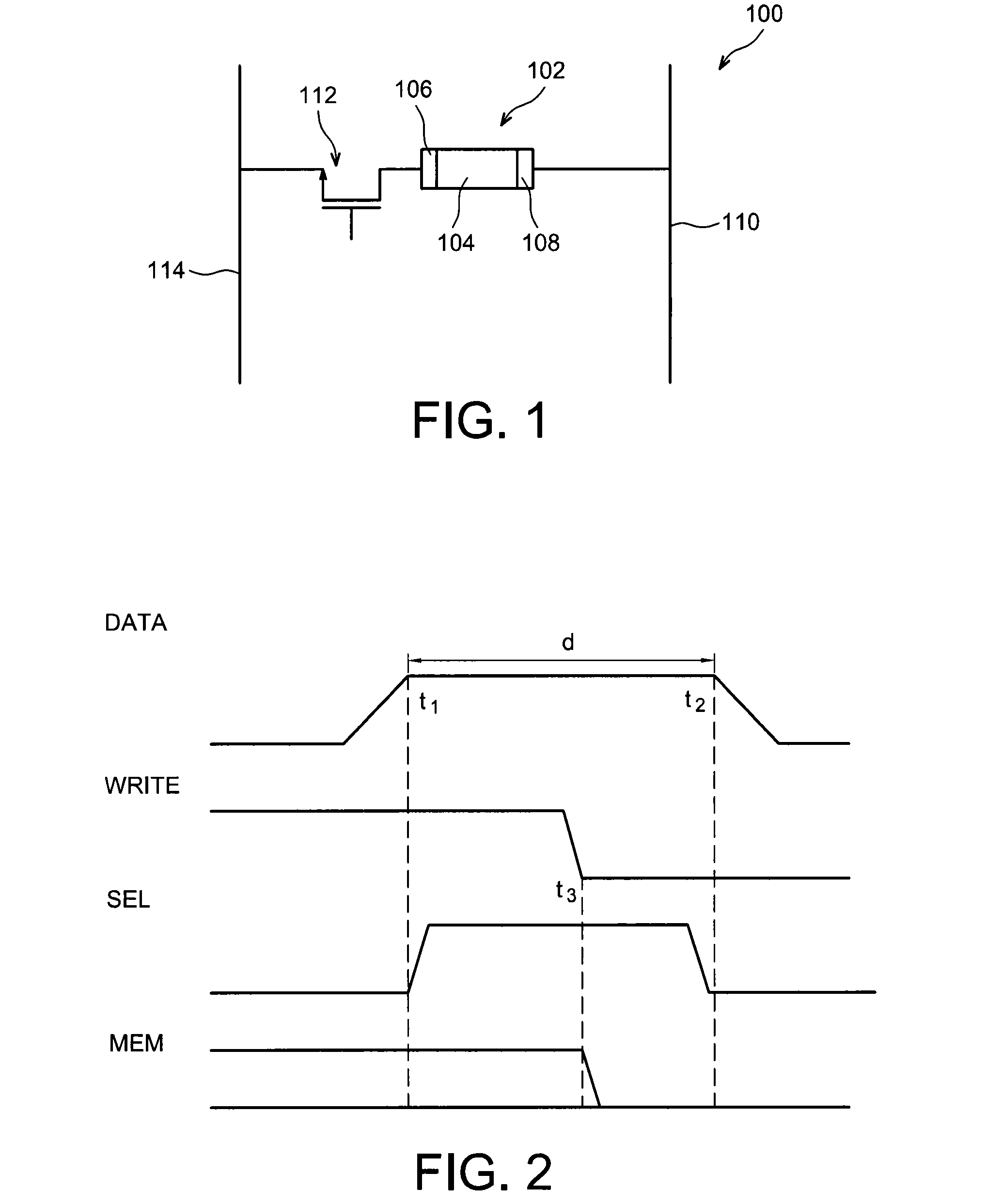
[0050]FIG. 1 shows an electronic circuit according to the invention, comprising a bipolar switching non-volatile memory device intended to be programmed by implementing a programming method also according to the invention,

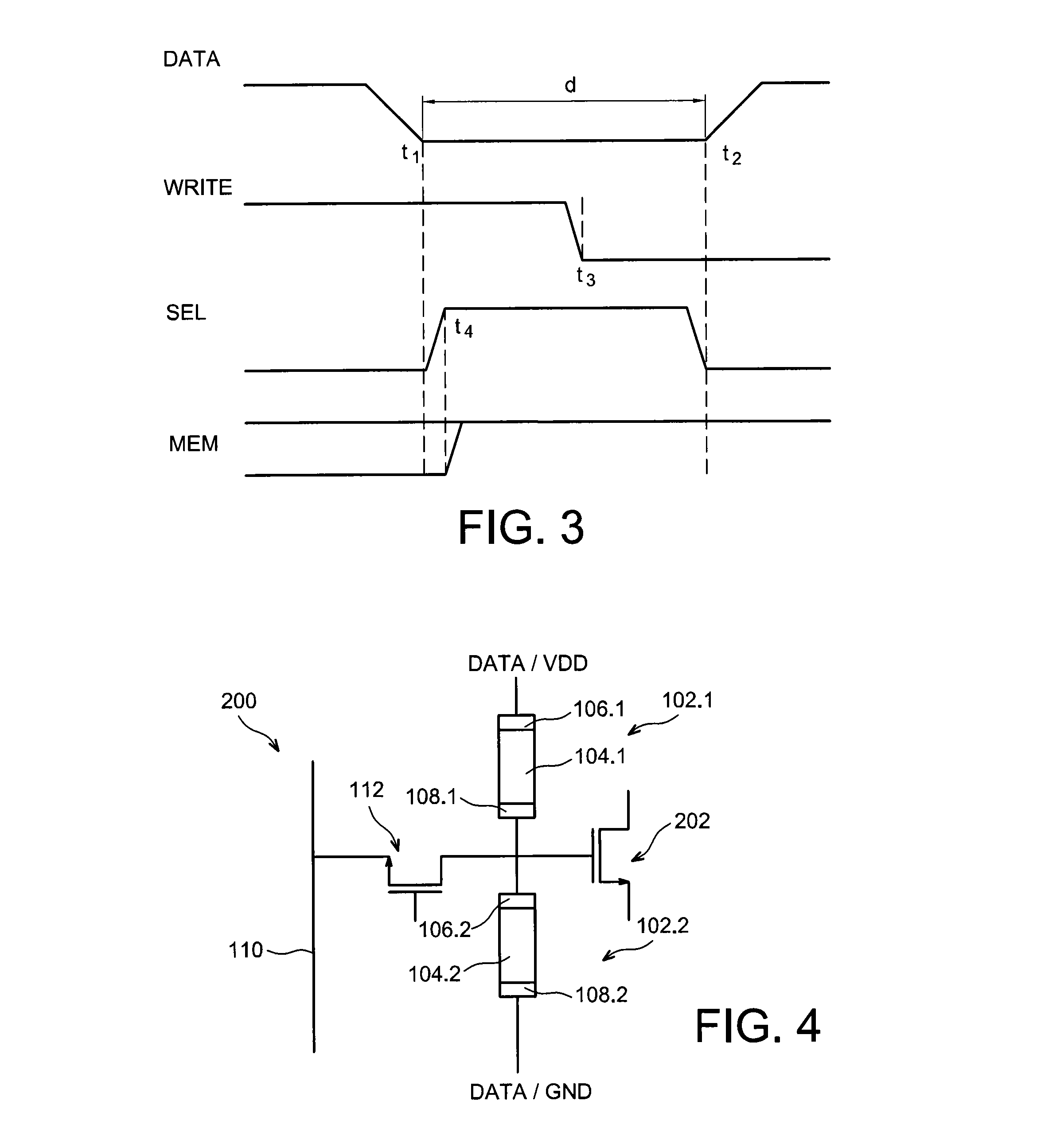
[0051]FIGS. 2 and 3 are chronograms for a memory device according to the first embodiment, obtained on implementing a programming method according to the invention,

second embodiment

[0052]FIG. 4 shows an electronic circuit according to the invention, comprising two bipolar switching non-volatile memory devices intended to be programmed in a complementary manner by implementing a programming method also according to the invention,

[0053]FIGS. 5 and 6 are chronograms for an electronic circuit according to the second embodiment of the invention, obtained on implementing a programming method for two memory devices, also subject to this invention,

third embodiment

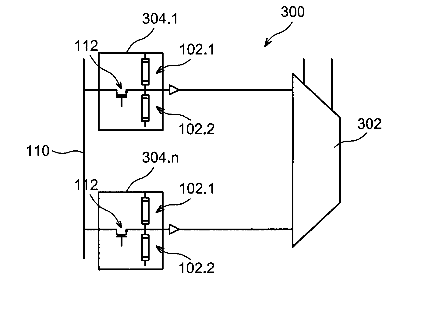
[0054]FIG. 7 shows an electronic circuit according to the invention, comprising multiple bipolar switching non-volatile memory devices intended to be programmed in a complementary manner and in twos, by implementing a programming method also according to the invention,


PUM


Abstract

An electronic circuit including a bipolar switching memory device including first and second electrodes at terminals of which a programming voltage can be applied, the circuit including: a first mechanism applying, to the first electrode, a data signal having, during a time period d, a constant state 0 or 1; a second mechanism applying, to the second electrode, a control signal that alternates, during time period d, between state 1 and state 0, the control signal being same regardless of the state in which the memory device is programmed; a selection device allowing a current to flow into the memory device during a programming time included in time period d; and a change of state of the control signal taking place during the programming time.

Description

TECHNICAL FIELD[0001]The invention relates to a method for programming at least one bipolar switching memory device, for example a CBRAM or RRAM device, as well as a method for programming a differential memory cell comprising at least two bipolar switching memory devices. The invention also relates to an electronic circuit comprising at least one bipolar switching memory device and designed to program the memory device.PRIOR ART[0002]Several types of non-volatile memories exist, for example magnetic memories (MRAM, STTRAM), phase change memories (PCRAM) or resistive memories (CBRAM, RRRAM or ReRAM, OxReRAM). These memories can store at least two different states in a non-volatile manner. These memories are either unipolar, i.e. they can be programmed in either of the two memory states by applying different value writing voltages or currents, however with the same polarity, or bipolar, i.e. they can be programmed in either of the two memory states by applying writing voltages or cur...

Claims


Application Information

Patent Timeline
Patent Type & Authority Applications(United States)
IPC IPC(8): G11C13/00H03K3/356
CPCG11C13/0007G11C13/0011G11C13/0061G11C13/0069G11C14/009G11C2013/0073G11C2213/78G11C2213/79G11C2213/82H03K3/356
Inventor ONKARAIAH, SANTHOSHBELLEVILLE, MARCCLERMIDY, FABIEN
Owner COMMISSARIAT A LENERGIE ATOMIQUE ET AUX ENERGIES ALTERNATIVES
Why Eureka
Try Eureka