Display device and method for driving same

a technology of a display device and a drive device, which is applied in the field of display devices, can solve the problems of affecting the performance the inability to achieve large size and high definition, and the tendency to vary the threshold voltage, so as to prevent the occurrence of length variations, effectively compensate for the degradation of the drive transistor, and the effect of length

Active Publication Date: 2015-12-31
SHARP KK
View PDF9 Cites 54 Cited by
  • Summary
  • Abstract
  • Description
  • Claims
  • Application Information

AI Technical Summary

Benefits of technology

[0121]According to the first aspect of the present invention, in a display device including a pixel circuit that includes an electro-optic element (e.g., an organic EL element) whose luminance is controlled by a current and a drive transistor configured to control a current to be supplied to the electro-optic element, detection of a characteristic of the drive transistor and detection of a characteristic of the electro-optic element are performed. Then, a video signal is corrected by use of correction data obtained in consideration of detection results of both the drive transistor and the electro-optic element. Since a data signal based on the video signal corrected in this manner is supplied to the pixel circuit, a drive current with such magnitude as to compensate for the degradation of the drive transistor and the degradation of the electro-optic element is supplied to the electro-optic element. Here, detection of the characteristic of the electro-optic element is performed during a light emission period of the electro-optic element. This prevents the length of the light emission period from becoming shorter than the length of the conventional light emission period due to the detection of the characteristic of the drive transistor and the electro-optic element. Thus, it is possible to simultaneously compensate for both degradation of the drive transistor and degradation of the electro-optic element without causing special light emission at the time of detecting characteristics in a display device.
[0122]According to the second aspect of the present invention, the length of the selection period of a monitor row (row on which the characteristic is detected in each frame) is longer than the length of the selection period of a non-monitor row. Then, detection of the characteristic of the drive transistor is performed in that selection period. Hence a period for detecting the characteristic of the drive transistor is sufficiently ensured.
[0123]According to the third aspect of the present invention, both detection of the characteristic of the drive transistor and detection of the characteristic of the electro-optic element are performed during the light emission period of the electro-optic element. Therefore, differently from the configuration where detection of the characteristic is also performed during the selection period, the selection period of the monitor row is not required to be made long. This ensures the light emission period with a sufficient length. Further, this prevents occurrence of variations in length of the selection period depending on the row. As described above, in the display device, it is possible to simultaneously compensate for both the degradation of the drive transistor and the degradation of the electro-optic element without causing special light emission at the time of detecting characteristics, while sufficiently ensuring the light emission period without occurrence of variations in length of the selection period.
[0124]According to the fourth aspect of the present invention, a constant current is supplied to the electro-optic element which is subjected to detection of the characteristic. Therefore, by adjusting the time for supplying the constant current to the electro-optic element, it is possible to make the electro-optic element emit light with a desired luminance.
[0125]According to the fifth aspect of the present invention, it is possible to make the electro-optic element emit light with a desired luminance while detecting the characteristic of the electro-optic element.
[0126]According to the sixth aspect of the present invention, since a plurality of characteristics are detected as the characteristics of the electro-optic element, it is possible to more effectively compensate for the degradation of the drive transistor.

Problems solved by technology

As for an organic EL display device employing the passive matrix system, its structure is simple, but a large size and high definition are difficult to achieve.
However, regarding the thin film transistor, variations in threshold voltage tend to occur.
When variations in threshold voltage occur in the drive transistor provided in the display portion, variations in luminance occur, and the display quality thus deteriorates.
However, as for the organic EL element, current efficiency decreases with the lapse of time.
This results in occurrence of burning.

Method used


Image

  • Display device and method for driving same
  • Display device and method for driving same
  • Display device and method for driving same

Examples


first embodiment

1. First Embodiment

1.1 Whole Configuration

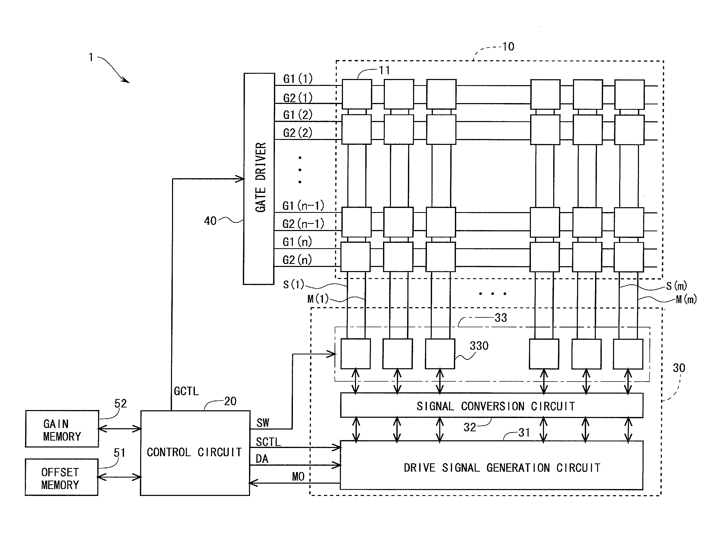
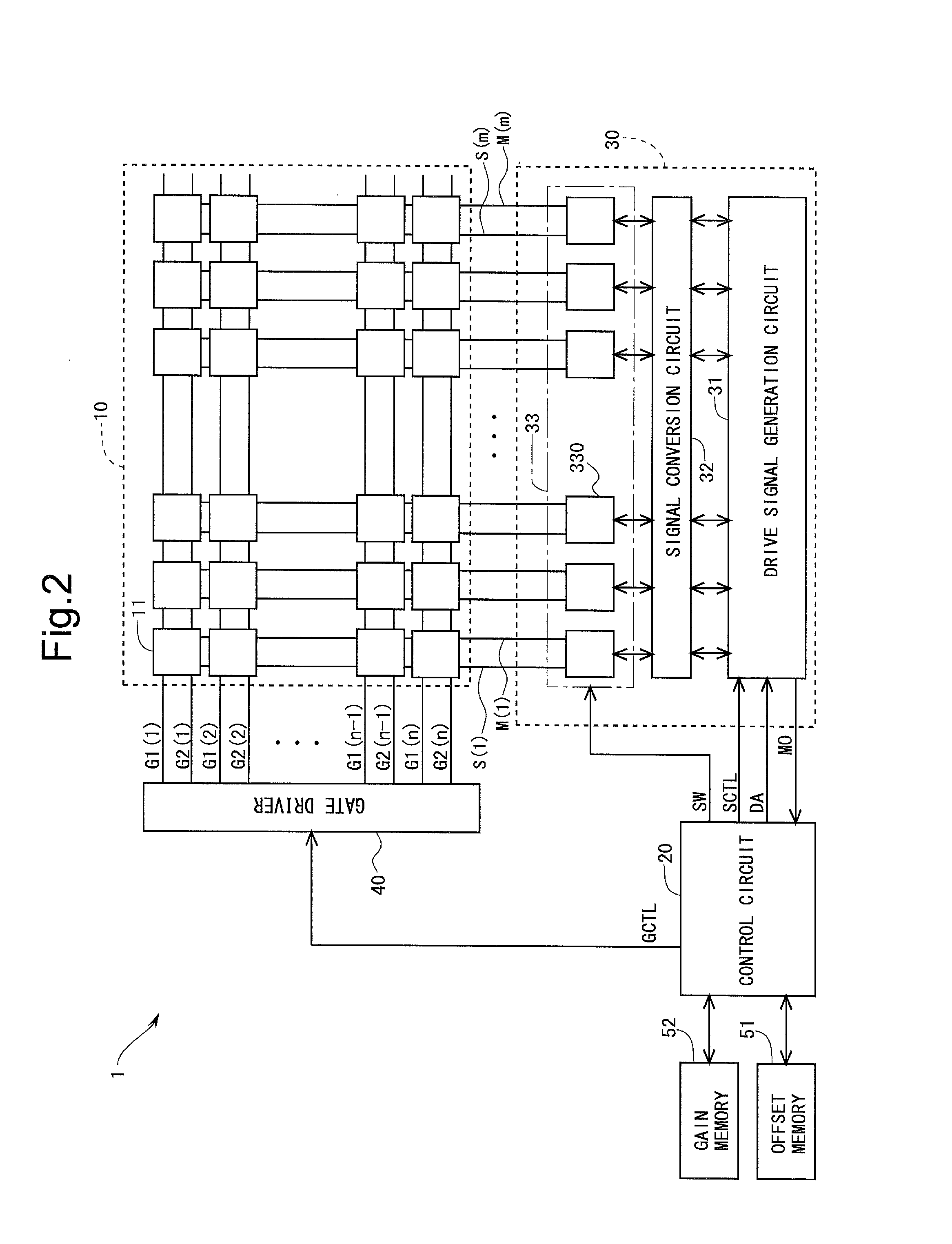
[0195]FIG. 2 is a block diagram showing a whole configuration of an active matrix-type organic EL display device 1 according to a first embodiment of the present invention. This organic EL display device 1 is provided with a display portion 10, a control circuit 20, a source driver (a data line drive circuit) 30, a gate driver (a scanning line drive circuit) 40, an offset memory 51, and a gain memory 52. It is to be noted that one or both of the source driver 30 and the gate driver 40 may be configured to be integrally formed with the display portion 10. Further, the offset memory 51 and the gain memory 52 may be physically formed of one memory.

[0196]It should be noted that the pixel circuit drive portion is realized by the source driver 30 and the gate driver 40, and the correction data storage portion is realized by the offset memory 51 and the gain memory 52, in the present embodiment.

[0197]The display portion 10 is provided with m data l...

second modified example

1.5.2 Second Modified Example

[0250]In the first embodiment, the monitor line M is configured to connect to either the current measurement portion 38 or the voltage measurement portion 39 as shown in FIG. 7. However, the present invention is not restricted to this, and it is also possible to employ a configuration where the monitor line M can be brought into the high impedance state (configuration of the present modified example).

[0251]FIG. 24 is a diagram showing a configuration in the vicinity of one end of the monitor line M in the present modified example. As grasped from FIG. 24, the monitor line M is brought into any of the state of being connected to the current measurement portion 38, the state of being connected to the voltage measurement portion 39 and the high impedance state by the switching control signal SW, in the present modified example.

[0252]Incidentally, in the first embodiment, concerning adjustment of the length of the light emission time of the organic EL elemen...

third modified example

1.5.3 Third Modified Example

[0253]In the first embodiment, the description has been given on the premise that one monitor circuit 322 including the current measurement portion 38 and the voltage measurement portion 39 is provided for one column. However, the present invention is not restricted to this, and it is also possible to employ a configuration where one monitor circuit 322 is shared by a plurality of columns (configuration of the present modified example).

[0254]In the present modified example, similarly to the second modified example (see FIG. 24), the monitor line M is brought into any of the state of being connected to the current measurement portion 38, the state of being connected to the voltage measurement portion 39, and the high impedance state. Further, in the present modified example, the vicinity of one end of the monitor line M has a configuration shown in FIG. 25. That is, one monitor circuit 322 is provided for each K monitor lines M.

[0255]In such a configuratio...


PUM


Abstract

Provided is a driving method whereby it is possible to simultaneously compensate for both degradation of a drive transistor and degradation of a light-emitting element without causing special light emission at the time of detecting characteristics in a display device. In a display device which includes a pixel circuit including an electro-optic element and a drive transistor, a driving method includes: a first characteristic detection step for detecting a characteristic of the drive transistor; a second characteristic detection step for detecting a characteristic of the electro-optic element; a correction data storage step for storing characteristic data obtained based on detection results in the first and second characteristic detection steps as correction data; and a video signal correction step for correcting the video signal based on the correction data. The second characteristic detection step is performed in a light emission period.

Description

TECHNICAL FIELD[0001]The present invention relates to a display device and a method for driving the same, and more specifically to a display device provided with a pixel circuit including an electro-optic element such as an organic EL (Electra Luminescence) element, and a method for driving the same.BACKGROUND ART[0002]As a display element provided in a display device, there have hitherto been an electro-optic element whose luminance is controlled by an applied voltage, and an electro-optic element whose luminance is controlled by a flowing current. Examples of the electro-optic element whose luminance is controlled by an applied voltage include a liquid crystal display element. Meanwhile, examples of the electro-optic element whose luminance is controlled by a flowing current include an organic EL element. The organic EL element is also called an OLED (Organic Light-Emitting Diode). An organic EL display device that uses the organic EL element being a spontaneous electro-optic elem...

Claims


Application Information

Patent Timeline
Patent Type & Authority Applications(United States)
IPC IPC(8): G09G3/34G09G3/32
CPCG09G3/3225G09G2300/0861G09G2320/041G09G2320/045H01L27/3241G09G3/3291G09G2320/0233G09G2300/043G09G2320/0276G09G3/3233G09G3/3283G09G2310/08G09G3/3406G09G2320/0295H10K59/10
Inventor KISHI, NORITAKA
Owner SHARP KK
Why Eureka
Try Eureka