Immittance conversion circuit and filter

a conversion circuit and filter technology, applied in the field of two-terminal immittance circuits, can solve the problems of loss, performance and the range of use of the circuit, and adversely affect the function value generated at the function generation terminal,

Active Publication Date: 2015-12-31
MARCDEVICES
View PDF2 Cites 1 Cited by
  • Summary
  • Abstract
  • Description
  • Claims
  • Application Information

AI Technical Summary

Benefits of technology

[0018]According to one embodiment of the present invention, a bid

Problems solved by technology

Due to close electrical coupling between the function generation terminals and the function control terminal, a signal applied to the function control terminal may adversely affect the function value generated at the function generation terminals.
As a result, performance and the range of use thereof are limited compared with a general bidirectional two-terminal passive component having no electrical

Method used


Image

  • Immittance conversion circuit and filter
  • Immittance conversion circuit and filter
  • Immittance conversion circuit and filter

Examples


embodiment 1

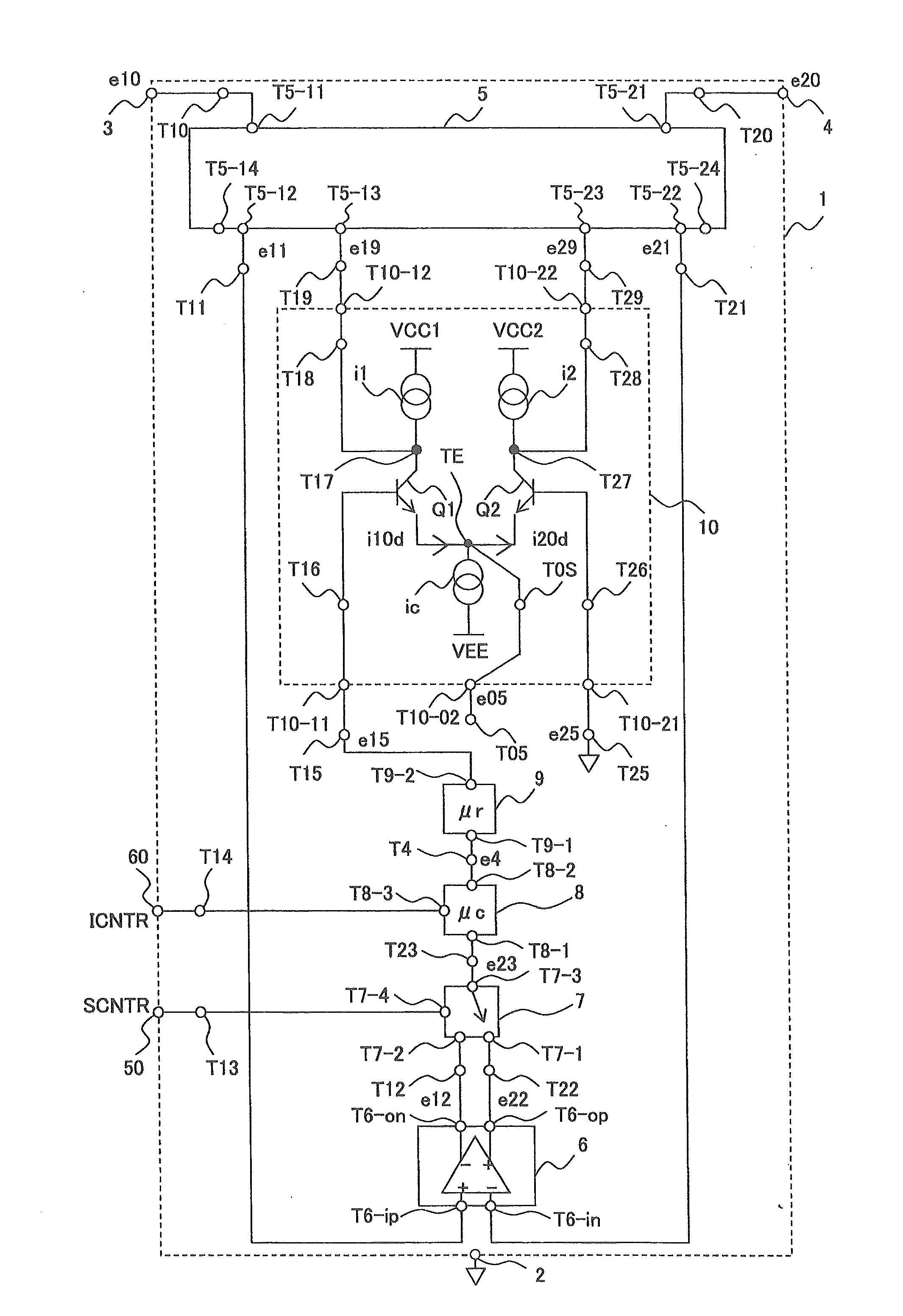
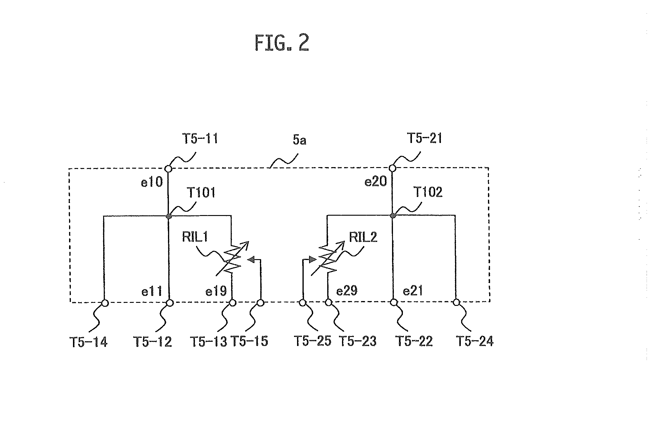
[0043]In the first embodiment, with reference to FIG. 1, detailed description is given of the example of using the impedance conversion generation circuit 5a shown in FIG. 2 as the immittance conversion generation circuit 5 included in the bidirectional floating immittance conversion circuit 1. In the first embodiment, the circuit shown in FIG. 3 is used as the conversion target circuit 9.

[0044]The bidirectional floating immittance conversion circuit 1 includes a reference terminal 2, a first terminal 3, a second terminal 4, a sign switching control input terminal 50, an immittance level control input terminal 60, the immittance conversion generation circuit 5, a difference signal detection circuit 6, a signal sign switching circuit 7, the conversion target circuit (origin circuit) 9, and an immittance conversion drive circuit 10.

[0045]The immittance conversion generation circuit 5 divides a signal e10 inputted to a terminal T5-11 through a terminal T10 from the first terminal 3, an...

embodiment 2

[0137]In the first embodiment, the description is given of the case where the conditions of Formula (3) are satisfied when the value of the total gain μta is large. Ina second embodiment, description is given of a bidirectional floating immittance conversion circuit 1 in the case where the value of the total gain μta extensively changes, i.e., a correspondence relationship between the two-terminal impedance z0 and the total gain μta of the conversion target circuit always includes the same constant term element for all elements in the coefficient matrix on the right-hand side of Formula (2) even if the value of the total gain μta is small.

[0138]In order to achieve such an effect, a predetermined correction signal from a signal correction circuit (also called an immittance conversion control circuit) shown in FIG. 8 is supplied to the terminal T10-21 in the bidirectional floating immittance conversion circuit 1 shown in FIG. 1. As a result, the floating effect of the immittance conve...

embodiment 3

[0190]In a third embodiment, description is given of means for reducing unintended resistance components (loss) in the bidirectional floating immittance conversion circuit 1.

[0191]For example, in the case of aiming for a high resonance acutance (high Q value) as the total gain μta, unintended loss needs to be reduced. Also, for example, when reactance values are set for the first and second immittance level setting impedance elements RIL1 and RIL2, unintended loss needs to be reduced to realize pure reactance values.

[0192]In this case, a change is made also including the constant term ½ in the denominator on the right-hand side of Formula (9). In order to do this, a loss control circuit 21 may be added to the circuit shown in FIG. 1.

[0193]A method for adding the loss control circuit 21 is described using the loss compensation circuit 20 shown in FIG. 10. The loss compensation circuit 20 includes terminals T20-11, T20-21, T20-12, T20-22, T20-3, T20-4, T20-5 and T20-6. These eight ter...


PUM


Abstract

An immittance conversion circuit includes a first terminal and a second terminal, and includes: a conversion target circuit configured to amplify or attenuate a signal with desired frequency and gain characteristics, and output the resultant signal; a difference signal detection circuit configured to supply the input terminal of the conversion target circuit with a signal of a difference between signals generated at the first and second terminals; an immittance conversion drive circuit configured to perform differential output processing to generate a voltage of a difference between a correction voltage and the signal outputted from the conversion target circuit, and output feedback signals to an immittance conversion generation circuit; and the immittance conversion generation circuit having an immittance conversion generation action to generate, at each of the first and second terminals, a signal of currents or voltages of the corresponding inputted feedback signal and the signal inputted to the first or second terminal. A signal of a difference between the signals generated at the first and second terminals is inputted to the immittance conversion drive circuit as the correction voltage.

Description

CROSS-REFERENCE TO RELATED APPLICATION[0001]This application is based upon and claims the benefit of priority of International Application PCT / JP2013 / 052896, filed on Feb. 7, 2013, the entire contents of which are incorporated herein by reference.TECHNICAL FIELD[0002]The present invention relates to a two-terminal immittance circuit which takes on a value corresponding to a gain obtained by an electronic circuit, and more particularly relates to a bidirectional circuit having floating properties.BACKGROUND ART[0003]An electronic circuit generally includes a circuit composed of a combination of: bidirectional two-terminal passive components such as a resistor, and a coil and a capacitor; and unidirectional three-terminal active components such as transistors.[0004]In many cases, any of a resistive element, a capacitive element, an inductive element and the like, which are bidirectional two-terminal passive components, is a component for determining frequency characteristics of a circ...

Claims


Application Information

Patent Timeline
IPC IPC(8): H03H11/40
CPCH03H11/46H03H11/40
Inventor HIRAMA, KOICHI
Owner MARCDEVICES
Why Eureka
Try Eureka