Array substrate, liquid crystal display panel and display device

a liquid crystal display panel and array substrate technology, applied in semiconductor devices, optics, instruments, etc., can solve the problems of increasing process difficulty in manufacturing and increasing process difficulty in array substrate manufacturing, so as to reduce process difficulty in manufacturing array substrate, the effect of preventing the phenomenon of light leakag

Active Publication Date: 2016-01-14
BOE TECH GRP CO LTD
View PDF10 Cites 11 Cited by
  • Summary
  • Abstract
  • Description
  • Claims
  • Application Information

AI Technical Summary

Benefits of technology

[0008]Embodiments of the invention provide an array substrate, a liquid crystal display panel and a display device, which can effectively preve

Problems solved by technology

In a high resolution liquid crystal display device, since the pixel pitch of the array substrate is small, the wider the shield electrode is, the smaller the slit width of the common electrode, within one pixel pitch range, provided in the same layer as the shield electrode is, which will i

Method used


Image

  • Array substrate, liquid crystal display panel and display device
  • Array substrate, liquid crystal display panel and display device
  • Array substrate, liquid crystal display panel and display device

Examples


Embodiment Construction

[0024]The particular implementations of the array substrate, the liquid crystal display panel and the display device provided by the embodiments of the invention will be described in detail below in conjunction with the accompanying drawings.

[0025]Sizes and shapes of all parts in the drawings do not reflect the true scale of the array substrate, and are intended to just schematically illustrate the contents of the invention.

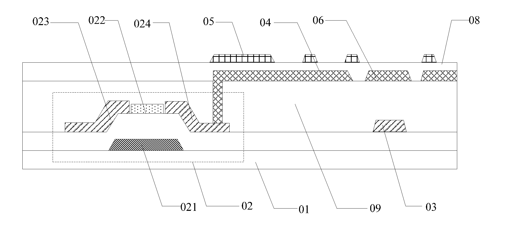
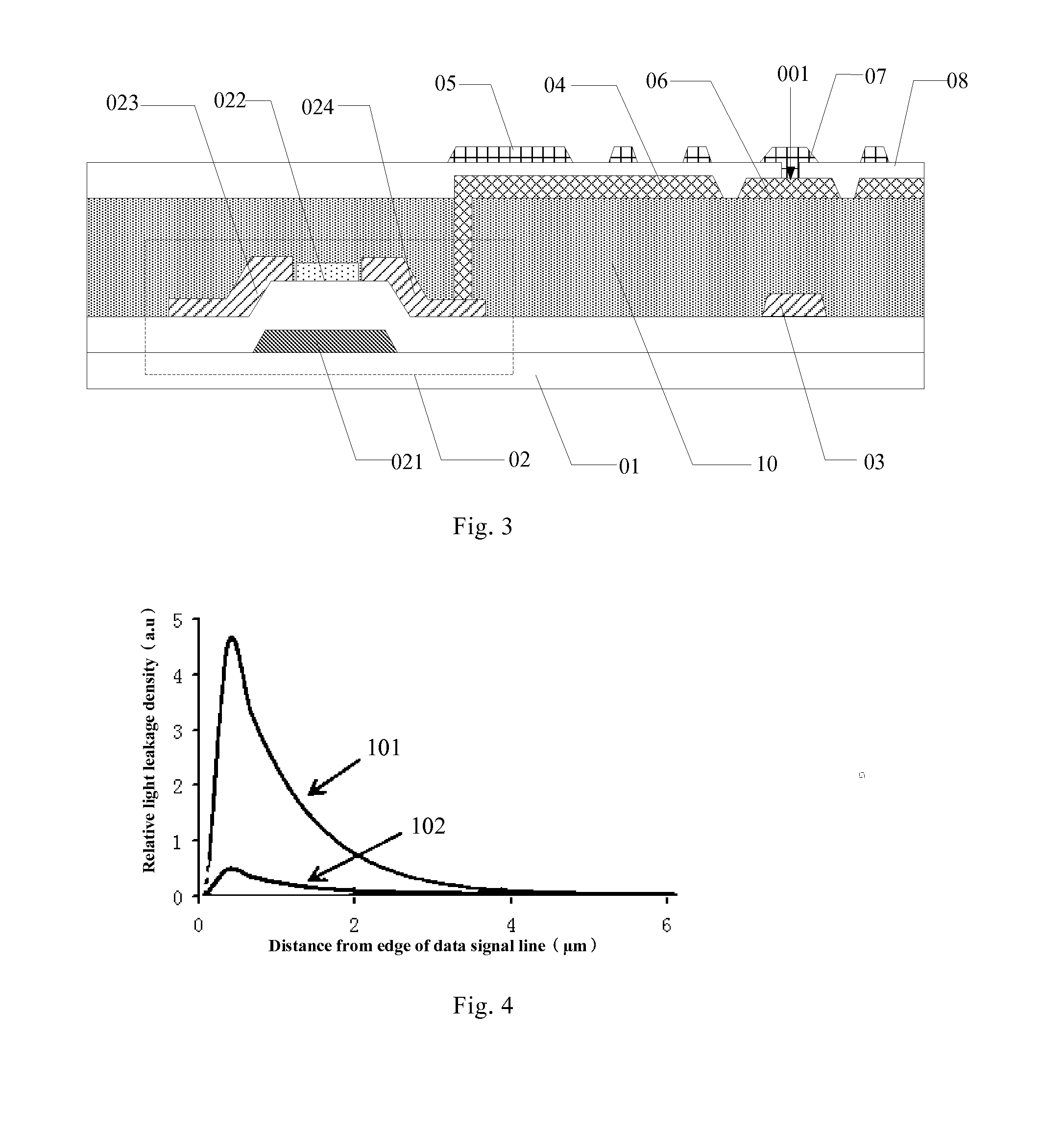
[0026]An embodiment of the invention provides an array substrate, as shown in FIGS. 2 and 3, and the array substrate includes a base substrate 01, a thin film transistor 02 and a data signal line 03 provided on the base substrate 01, as well as a pixel electrode 04 and a common electrode 05 which are successively provided above the thin film transistor 02 and are insulated from each other, wherein the thin film transistor 02 includes a gate electrode 021, an active layer 022, a source electrode 023, and a drain electrode 024, the source electrode 023, the drain e...


PUM


Abstract

The invention discloses an array substrate, a liquid crystal display panel and a display device, since the first shield electrode, which intents to shield instantaneous electromagnetic signals in a data signal line, and a pixel electrode are provided in the same layer, compared to the existing array substrate in which the shield electrode and a common electrode are provided in the same layer, since the pixel electrode is closer to the data signal line, through the first shield electrode, the light leakage phenomenon can be effectively prevented from occurring in the array substrate, and the color mixing phenomenon of the array substrate can be alleviated, and further the distance between the first shield electrode provided in the same layer as the pixel electrode and the data signal line can be decreased, and the width of the first shield electrode is decreased.

Description

Field of the Invention[0001]The present invention relates to the field of display technology, in particular to an array substrate, a liquid crystal display panel and a display device.BACKGROUND OF THE INVENTION[0002]Liquid crystal display technology is developing rapidly, and becomes a new star in industry and a highlight in economic development. In the vigorous development of liquid crystal display technology, wide viewing angle, high display quality and fast response speed etc. become urgent requirements on a liquid crystal display device. At present, Advanced Super Dimension Switch (ADSDS, abbreviated as ADS) type liquid crystal display technology has become a research hotspot in recent years due to its wide viewing angle, high display quality and fast response speed etc.[0003]In an ADS liquid crystal display technology, a multidimensional electric field is formed of an electric filed formed between edges of slit-shaped electrodes in the same layer and an electric field formed be...

Claims


Application Information

Patent Timeline
IPC IPC(8): G02F1/1343G02F1/1333G02F1/1362G02F1/1368
CPCG02F1/134309G02F1/1368G02F2001/136218G02F1/133345G02F1/136227G02F1/136286G02F1/134318G02F1/134372G02F1/136218
Inventor CHOI, HYUNSIC
Owner BOE TECH GRP CO LTD
Why Eureka
Try Eureka