Anti-interference touch display panel

a touch display panel and display panel technology, applied in the field of touch display panels, can solve the problems of reducing product yield, adjacent touch-sensing units being easily short-circuited, and conventional touch-sensing structures, so as to enhance display performance, increase pixel aperture ratio, and avoid short-circuite

Inactive Publication Date: 2016-02-04
HANNSTAR DISPLAY NANJING +1
View PDF4 Cites 2 Cited by
  • Summary
  • Abstract
  • Description
  • Claims
  • Application Information

AI Technical Summary

Benefits of technology

[0032]Besides, because the pixel electrode and the data lines are disposed on the gate insulating layer in this invention, the pixel electrode can directly contact the drain instead of through the via for electrically connecting to the drain, and the pixel aperture ratio can be increased thereby. Furthermore, in the design of the common electrode of this invention, the consideration needn't be given to the interval between the common electrode and the gate line, so that the pixel aperture ratio won't be sacrificed.
[0033]Furthermore, the first anti-interference spots and / or the touch-sensing units are disposed corresponding to the light-blocking array layer (or the light-blocking layer), and for example, the light-blocking array layer is disposed corresponding to the first anti-interference spots. Thereby, the light-blocking array layer can not only define the position of the pixel but also block the light passing through the first anti-interference spots, so as to enhance the display performance.
[0034]In addition, this invention also discloses the replacement or sharing of some layers of the anti-interference touch display panel for the touch-sensing units. For example, the first conducting wire can act as the light-blocking layer or the first touch-sensing layer acts as the light-blocking layer. Thereby, the anti-interference touch display panel can be given the effects of decreasing the cost and the thickness.
[0035]Moreover, the shielding layer is disposed between the touch-sensing units and the display functional layer (e.g. liquid crystal layer) to prevent the electric field within the liquid crystal layer from affecting the touch-sensing units.
[0036]Besides, because the light-blocking array layer matches the metal mesh sensing units in shape and covers the metal mesh sensing units in this invention, the Moire phenomenon can be reduced.
[0037]In addition, the insulating layer of this invention possesses the anti-glare ability so that is can absorb and filter the external incident light. Thereby, the reflection and interference generated between the external incident light and the metal mesh can be reduced, the brightness contrast of the display panel can be enhanced, and the anti-glare effect can be provided against the external incident light.

Problems solved by technology

However, the conventional touch-sensing structures suffer the problem of a decreasing product yield.
However, because the interval between the touch-sensing units is just 10 μm˜30 μm, the adjacent touch-sensing units will be easily short-circuited when particles fall down or scratches happen during the process, or the touch-sensing units are bent.
As a result, the malfunction of the touch product may happen and the product yield will be decreased.

Method used


Image

  • Anti-interference touch display panel
  • Anti-interference touch display panel
  • Anti-interference touch display panel

Examples


Embodiment Construction

[0055]The present invention will be apparent from the following detailed description, which proceeds with reference to the accompanying drawings, wherein the same references relate to the same elements.

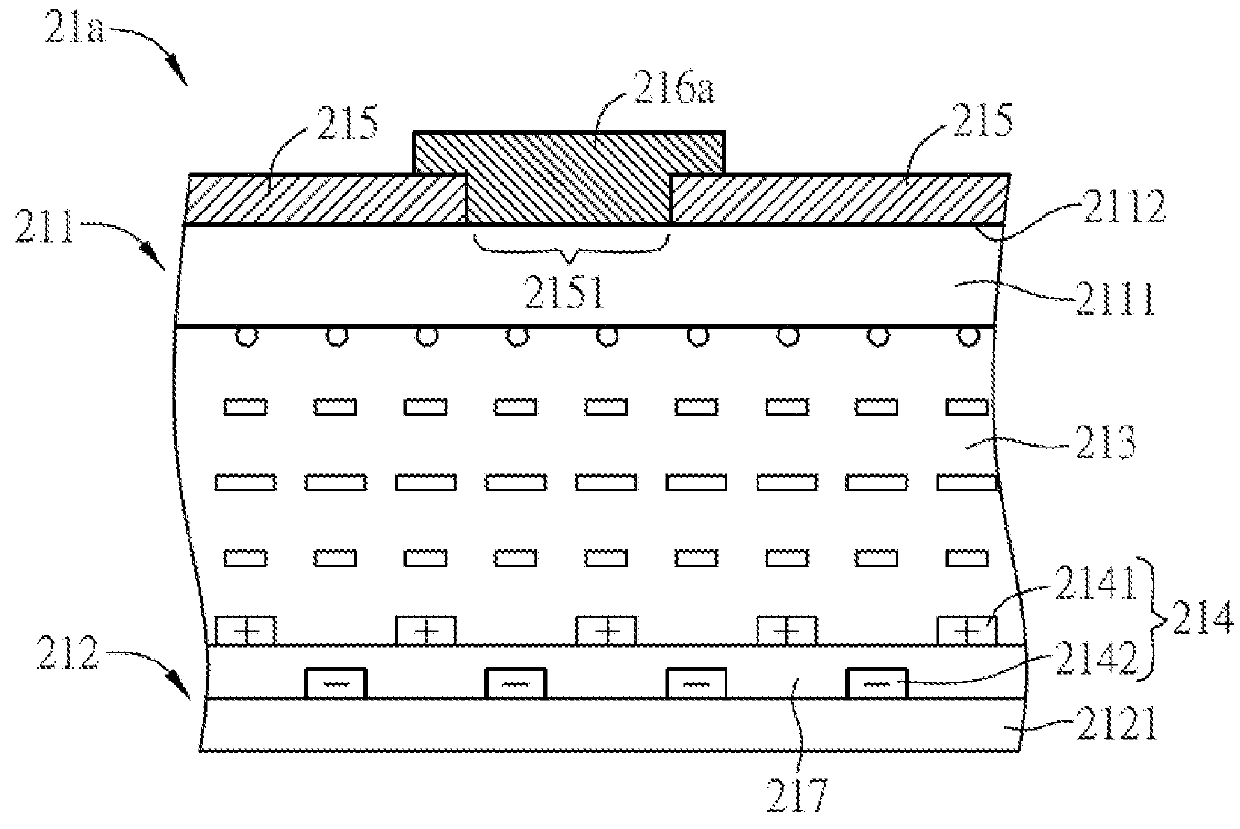
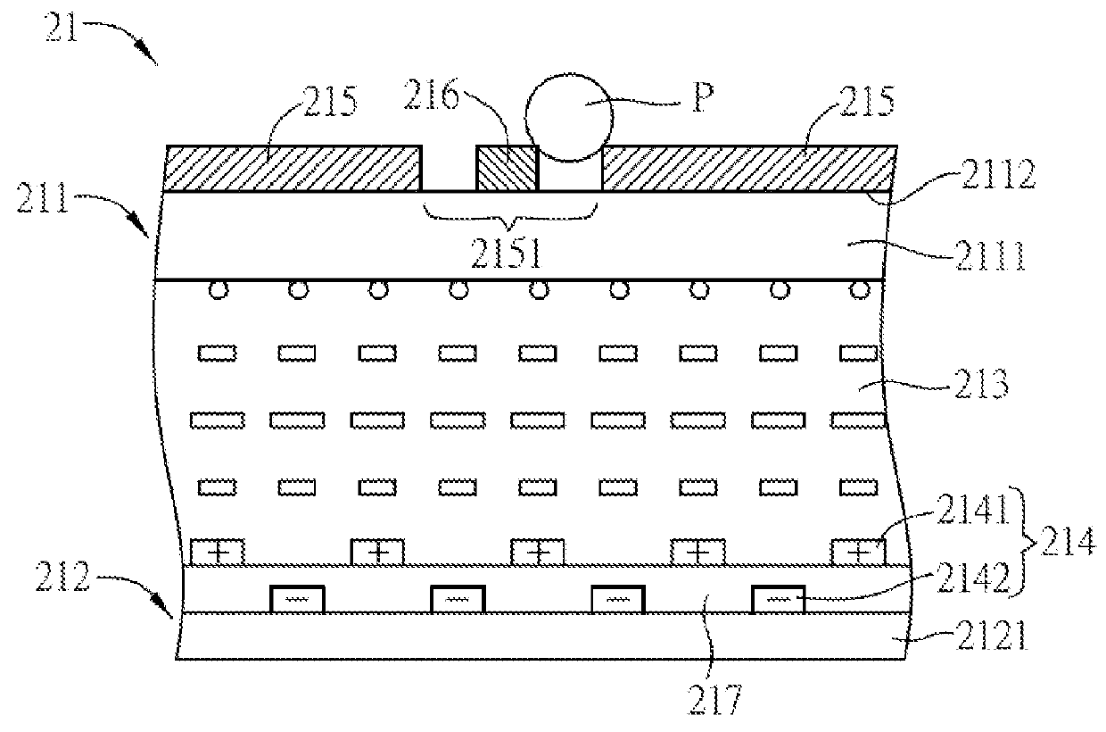
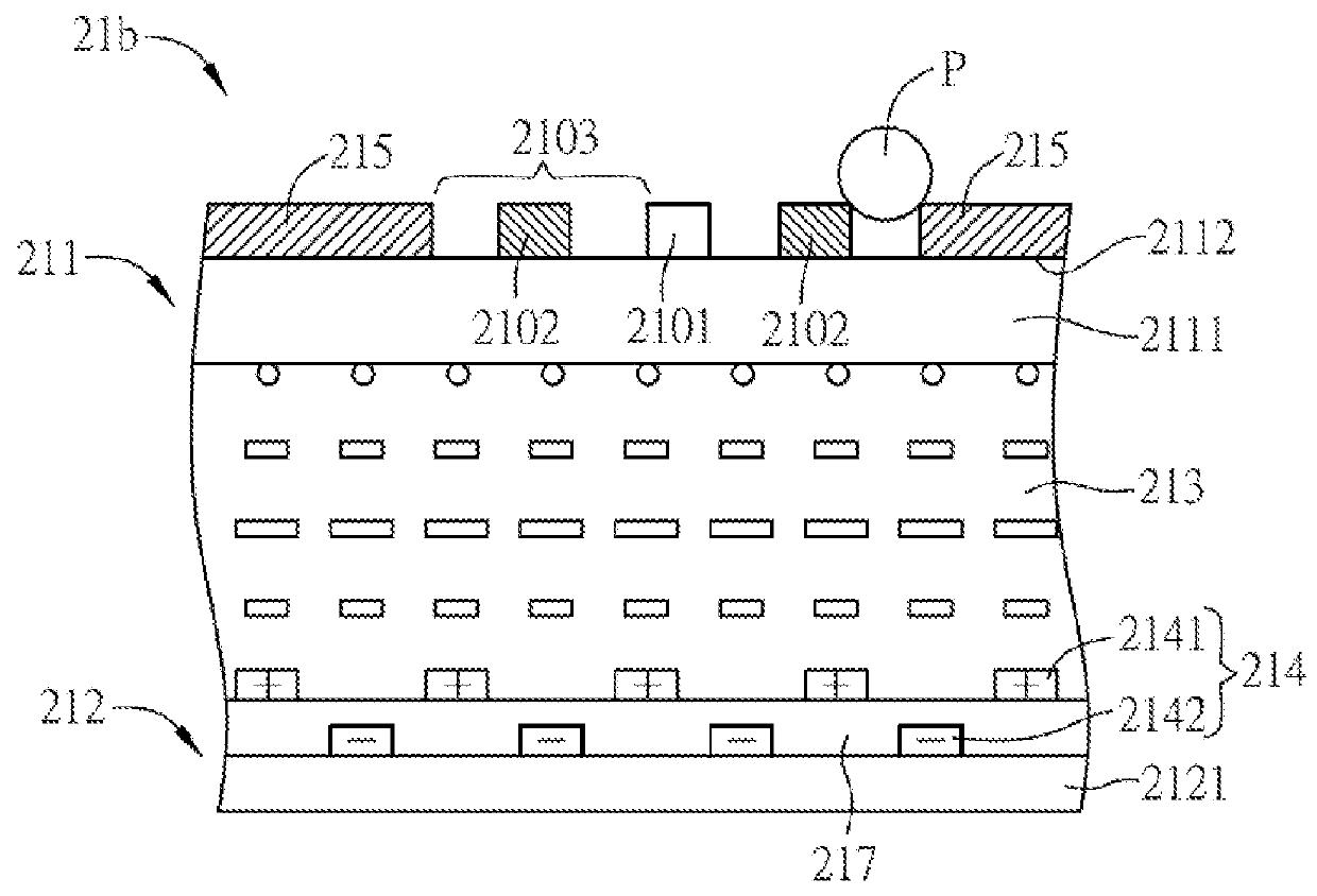
[0056]FIG. 1 is a schematic diagram of an anti-interference touch display panel 21 of an embodiment of the invention, and the anti-interference touch display panel 21 of this embodiment is illustrated as a FFS liquid crystal touch display panel for example. As shown in FIG. 1, the anti-interference touch display panel 21 comprises a color filter substrate 211, an active matrix transistor substrate 212, a display functional layer 213, an electrode pair 214, a plurality of touch-sensing units 215 and at least one anti-interference spot 216.

[0057]The color filter substrate 211 comprises a transparent substrate 2111, and can further comprise a color filter layer, or a black matrix layer, or an alignment layer, or a polarizing layer or other functional layers. Since the conventional art ca...


PUM


Abstract

An anti-interference touch display panel comprises a color filter substrate, an active matrix transistor substrate, a display functional layer, a plurality of touch-sensing units and at least one first anti-interference spot. The active matrix transistor substrate is disposed corresponding to the color filter substrate. The display functional layer is disposed between the color filter substrate and the active matrix transistor substrate. The touch-sensing units are coplanarly disposed on the color filter substrate, and a first interval region is formed between the adjacent-touch sensing units. The first anti-interference spot is disposed within the first interval region.

Description

CROSS REFERENCE TO RELATED APPLICATIONS[0001]This Non-provisional application claims priority under 35 U.S.C. §119(a) on Patent Application No(s). 201410365821.5, 201410367943.8, 201410367533.3, 201410366322.8 and 201410368046.9 filed in People's Republic of China on Jul. 29, 2014, the entire contents of which are hereby incorporated by reference.BACKGROUND OF THE INVENTION[0002]1. Field of Invention[0003]This invention relates to a touch display panel and, in particular, to an anti-interference touch display panel.[0004]2. Related Art[0005]Recently, the touch technology has been widely applied to common consumer electronic products, such as liquid crystal display (LCD) panels. The touch technology can be applied to the display panel in multiple types. For example, a touch panel is attached to the display panel, i.e. the out-cell type, or the touch-sensing units are directly formed on the display panel, which is the embedded type and can be divided into the on-cell type and the in-c...

Claims


Application Information

Patent Timeline
Patent Type & Authority Applications(United States)
IPC IPC(8): G06F3/041
CPCG06F3/041G06F3/0412G06F2203/04103G06F2203/04111G06F3/0443G06F3/0445G06F3/0446G06F3/0448
Inventor LEE, HSING-YINGTANG, DA-CHINGLU, TIEN-RONG
Owner HANNSTAR DISPLAY NANJING
Why Eureka
Try Eureka