
Eureka
For R&D, Eureka makes reading and utilizing patents & technical documents easy.
Eureka AIR
Designed for self-driven R&D workflows. Generate viable solutions, solve complex R&D challenges, empower your innovation with AI.

Eureka Materials
Designed for material experts only. Revolutionize your material R&D, from search, analyze, to developing new materials.

TechResearch
Generate reliable direction feasibility study reports for your R&D in just a few steps.

TechSeek
Discover and master advanced knowledge NOW. Basics, ideas, possibilities, all at once.

TechMind
As an expert in R&D Theories, TechMind can generates customized viable solutions instantly.

TechRisk
Analyze your overall solution with one click, know your potential R&D risks in advance.

TechMonitor
Get weekly tech updates, stay abreast of the latest tech innovations and key insights.
Imaging device and imaging system
- Summary
- Abstract
- Description
- Claims
- Application Information
AI Technical Summary
Benefits of technology
Problems solved by technology
Method used
Image

Examples
first embodiment
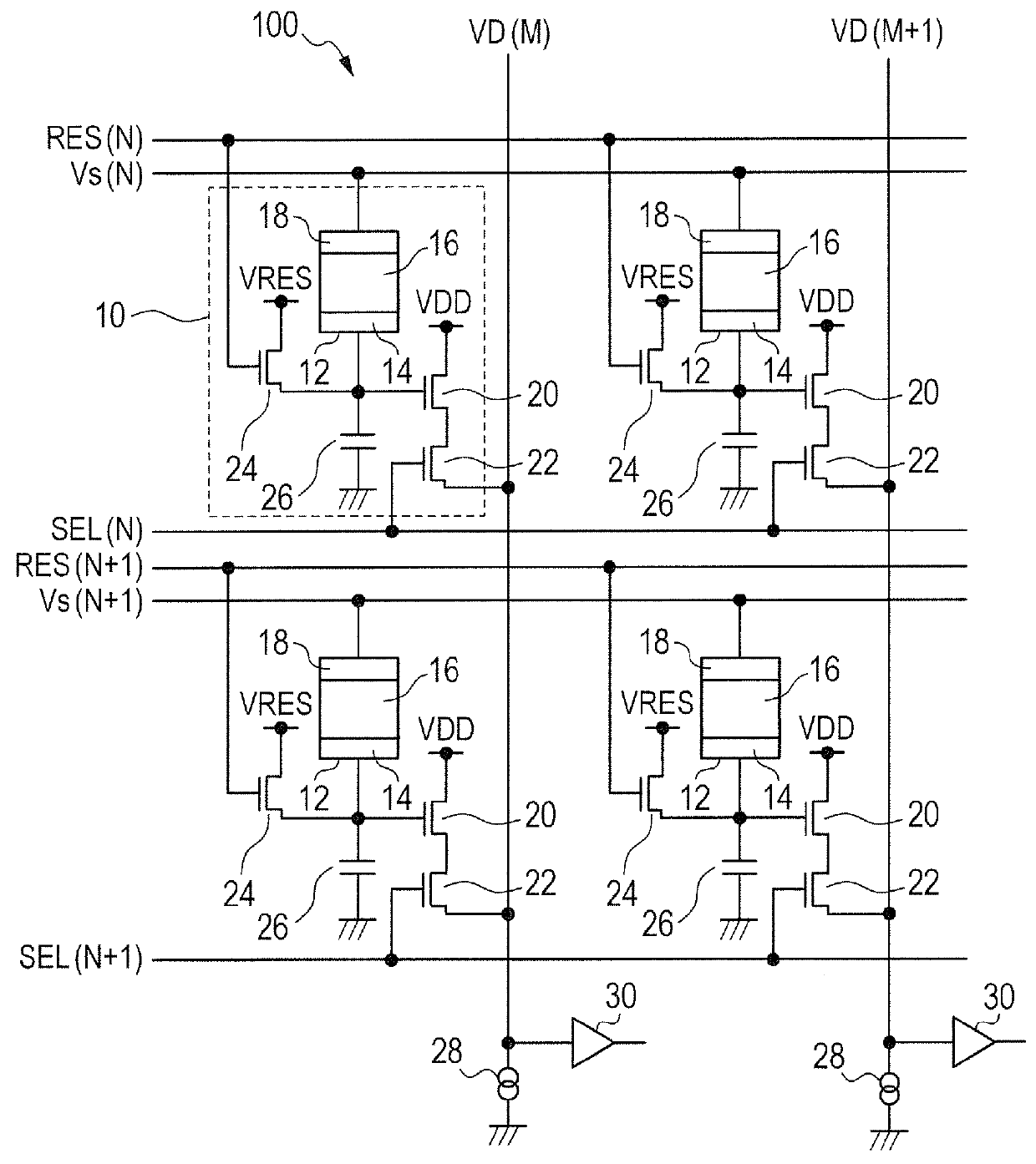
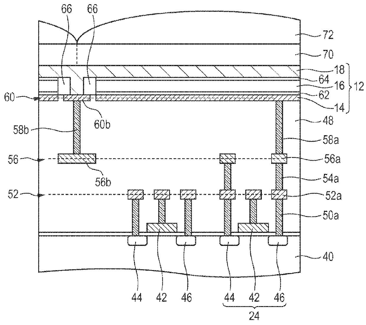
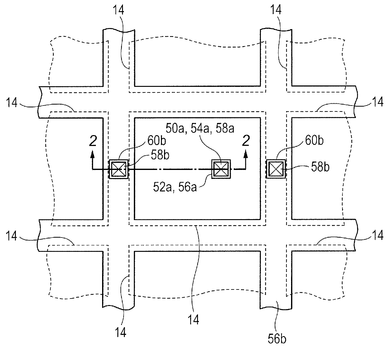
[0020]An imaging device according to a first embodiment of the present invention will be described with reference to FIGS. 1 to 5B.
[0021]FIG. 1 is a circuit diagram illustrating a pixel configuration of the imaging device according to the present embodiment. FIG. 2 is a schematic cross-sectional view illustrating a structure of the imaging device according to the present embodiment. FIG. 3 is a plan view schematically illustrating the structure of the imaging device according to the present embodiment. FIGS. 4A to 5B are schematic cross-sectional views illustrating a method of manufacturing the imaging device according to the present embodiment.
[0022]First, the pixel configuration of the imaging device according to the present embodiment will be described with reference to FIG. 1.
[0023]As illustrated in FIG. 1, an imaging device 100 according to the present embodiment includes a plurality of pixels 10 provided in a pixel region. The plurality of pixels 10 is arranged in a first dire...
second embodiment
[0067]An imaging device according to a second embodiment of the present invention will be described with reference to FIG. 6. FIG. 6 is a plan view illustrating a structure of the imaging device according to the present embodiment. The same constituent elements as those of the imaging device according to the first embodiment illustrated in FIGS. 1 to 5B are designated with the same reference signs, and the description will be omitted or simplified.
[0068]In the imaging device 100 according to the present embodiment, the Vs voltage line connected to the second electrode 18 is formed of two interconnection layers formed at different levels. More specifically, Vs voltage line 56c in a stripe pattern extending in a first direction is formed of the interconnection layer 56 as illustrated in FIG. 6. Vs voltage line 52c in a stripe pattern extending in a second direction intersecting the first direction is formed of the interconnection layer 52. Here, the first direction is the row directio...
third embodiment
[0073]An imaging device according to a third embodiment of the present invention will be described with reference to FIG. 7. FIG. 7 is a plan view illustrating a structure of the imaging device according to the present embodiment. The same constituent elements as those of the imaging device according to the first and second embodiments illustrated in FIGS. 1 to 6 are designated with the same reference signs, and the description will be omitted or simplified.
[0074]As in the second embodiment, the imaging device according to the present embodiment includes the Vs voltage line formed of the Vs voltage line 52c in a stripe pattern extending in the column direction and the Vs voltage line 56c in a stripe pattern extending in the row direction. The imaging device according to the present embodiment is different from the imaging device according to the second embodiment in that the contact portions of the Vs voltage line 52c, the voltage line 56c and the second electrode 18 are arranged in...
PUM
 Abstract
Description
Claims
Application Information
 - R&D Engineer
- R&D Manager
- IP Professional
- Industry Leading Data Capabilities
- Powerful AI technology
- Patent DNA Extraction
Browse by: Latest US Patents, China's latest patents, Technical Efficacy Thesaurus, Application Domain, Technology Topic, Popular Technical Reports.
© 2024 PatSnap. All rights reserved.Legal|Privacy policy|Modern Slavery Act Transparency Statement|Sitemap|About US| Contact US: help@patsnap.com