Fine-Grained Power Gating in FPGA Interconnects

a technology of fpga interconnects and fine-grained power, which is applied in the direction of power consumption reduction, logic circuit coupling/interface arrangement, pulse technique, etc., can solve the problems of increasing the cost (and, reducing the performance of the part without), and implementing a crossbar switch typically requires much more routing resources

Active Publication Date: 2016-02-04
RGT UNIV OF CALIFORNIA
View PDF4 Cites 7 Cited by
  • Summary
  • Abstract
  • Description
  • Claims
  • Application Information

AI Technical Summary

Problems solved by technology

For example, implementing a crossbar switch typically requires much more routing resources than a systolic array of the same gate count.
Since unused routing tracks increase the cost (and decrease the performance) of the part without providing any benefit, FPGA manufacturers try to provide just enough tracks so that most designs that will fit in terms of Lookup tables (LUTs) and IOs can be routed.
Indeed, such interconnect routing switches often comprise the majority of the silicon area on a FPGA and can be very power hungry, Static multiplexers are used within the interconnects to switch signals between wires.
When executing mapped designs, an FPGA can often have unused resources, resulting in current leakage.

Method used


Image

  • Fine-Grained Power Gating in FPGA Interconnects
  • Fine-Grained Power Gating in FPGA Interconnects
  • Fine-Grained Power Gating in FPGA Interconnects

Examples


Embodiment Construction

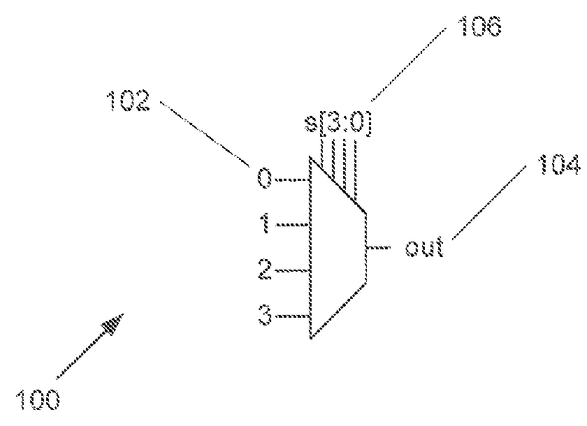
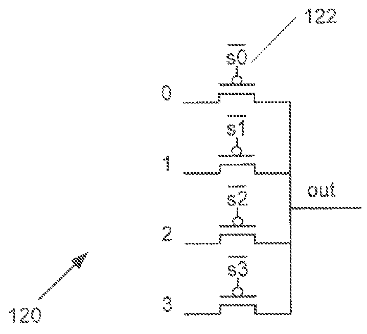
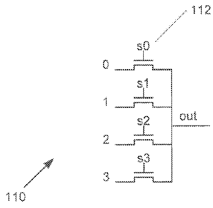
[0027]Turning now to the drawings, systems and methods for power gating in logic and / or computing circuitry employed for signal selection and routing in accordance with embodiments of the inventions are illustrated. In many embodiments, an N-input static multiplexer includes s[N-1:0] select-bits that control which input signal is passed to an inverter, In various embodiments, the N-input static multiplexer also includes an additional power gating enable input that can be selected to drive transistors. In an inverter stage of the N-input static multiplexer into cutoff and reducing leakage current without the need for a larger footer transistor. In several embodiments, power gating circuitry can be configured to achieve power gating of a N-input static multiplexer prior to the multiplexer initiating a power-on sequence to avoid the potential for the multiplexer to occupy a high power state prior to configuration as further discussed below.

[0028]In various embodiments, a static multipl...


PUM


Abstract

Systems and methods for power gating in logic and/or computing circuitry in accordance with embodiments of the inventions are disclosed. In one embodiment, a multiplexer for fine-grain power gating includes a first supply voltage and a second supply voltage, a plurality of inputs, a plurality of selection inputs, a selection circuitry configured to select one of the plurality of inputs, where one of the plurality of inputs is the first supply voltage and one of the selection inputs is a power gating enable input, an output inverter stage including a PMOS transistor and an NMOS transistor, where at least one input to the inverter stage is provided to the gates of the PMOS and NMOS transistors and selection of the power gating enable signal applies the first supply voltage to the gate of the PMOS transistor and places the PMOS transistor in a cutoff mode of operation.

Description

FIELD OF THE INVENTION[0001]The present inventions are directed to circuitry of and techniques for power reduction in logic and computing circuitry employed for signal selection and routing in circuitry including (but not limited to) processors, state machines, gate arrays, programmable gate arrays, field programmable gate arrays (FPGAs), and system-on-chips (SODS). For example, the systems and methods of the present inventions may be implemented in or for fine-grained power gating in FPGA interconnects. While the inventions and / or embodiments are often described below in the context of FPGA circuitry, such discussion, inventions and / or embodiments are also applicable to logic and / or computing circuitry including (but not limited to) processors, state machines, gate arrays, programmable gate arrays and SOCs. For the sake of brevity, a separate discussion for each and every logic and / or computing circuit is not provided with respect to each aspect of the disclosed invention; however ...

Claims


Application Information

Patent Timeline
Patent Type & Authority Applications(United States)
IPC IPC(8): H03K17/00H03K19/0185
CPCH03K19/018528H03K17/005H03K19/0016H03K19/09429H03K19/1737H03K19/17772
Inventor WANG, CHENGCHENGMARKOVIC, DEJAN
Owner RGT UNIV OF CALIFORNIA
Why Eureka
Try Eureka