Supercharge Your Innovation With Domain-Expert AI Agents!

Multiple input multiple output (MIMO) communication systems and methods for chip to chip and intrachip communication

Inactive Publication Date: 2016-02-04
QUALCOMM INC
View PDF5 Cites 6 Cited by
  • Summary
  • Abstract
  • Description
  • Claims
  • Application Information

AI Technical Summary

Benefits of technology

This patent describes a method and system for improving communication between chips and within a chip using multiple input multiple output (MIMO) techniques. The system models the communication channels as a matrix and evaluates the channel state information to determine the power constraint. A transfer function is then calculated to cancel out interference and crosstalk conditions. The transfer function is optimized to stay within the power constraint. The system also includes a control system that models the communication channels, evaluates the channel state information, and determines the power constraint. The transfer function is then calculated and applied to transmissions between the transmitter and receiver. The technical effect of this patent is to improve the efficiency and reliability of communication between chips and within a chip using MIMO techniques.

Problems solved by technology

Concurrent with the increases in complexity of the integrated circuits, there has been pressure to decrease the area consumed by the integrated circuits.
As the complexity of the integrated circuits increases, the number of conductive elements required to convey signals between the integrated circuits typically increases.
As the number of conductive elements increases and the frequencies increase, the opportunities for signals to interfere with one another increases.
If the EMI is too severe, undesirable errors may be introduced into the signal stream.

Method used


Image

  • Multiple input multiple output (MIMO) communication systems and methods for chip to chip and intrachip communication
  • Multiple input multiple output (MIMO) communication systems and methods for chip to chip and intrachip communication
  • Multiple input multiple output (MIMO) communication systems and methods for chip to chip and intrachip communication

Examples


Embodiment Construction

[0022]With reference now to the drawing figures, several exemplary aspects of the present disclosure are described. The word “exemplary” is used herein to mean “serving as an example, instance, or illustration.” Any aspect described herein as “exemplary” is not necessarily to be construed as preferred or advantageous over other aspects.

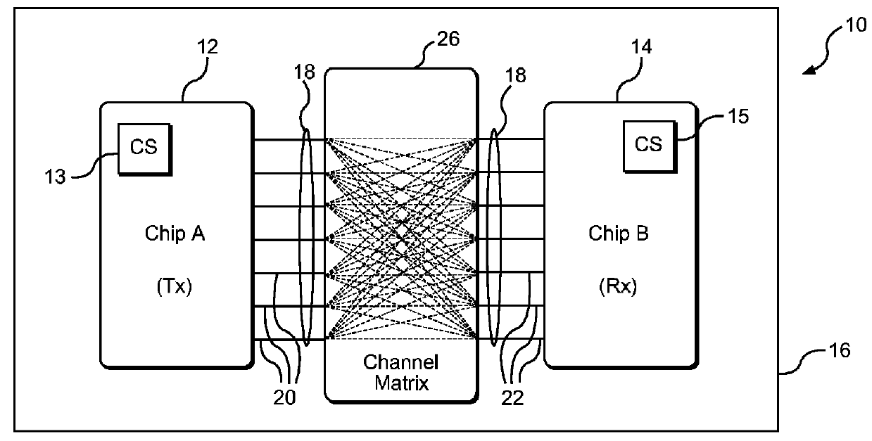
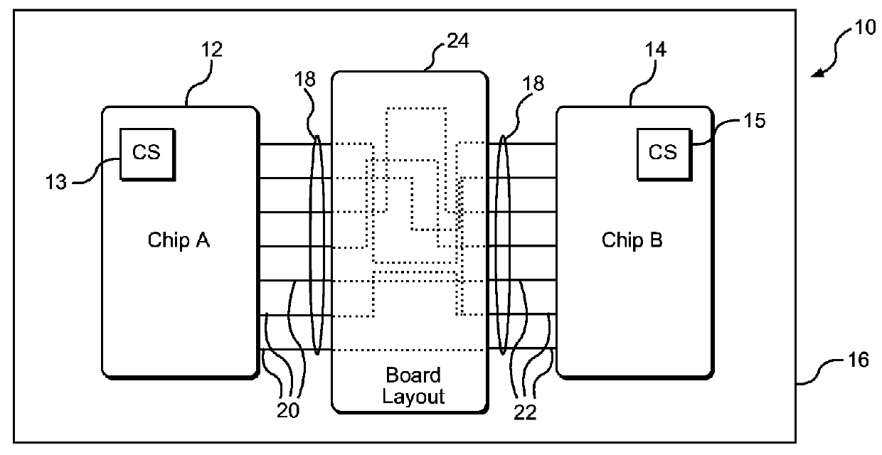
[0023]Aspects disclosed in the detailed description include multiple input multiple output (MIMO) communication systems and methods for chip to chip and intrachip communication. In exemplary aspects, MIMO techniques that have been applied to wireless communication systems are applied to interchip and intrachip communication systems. In particular, a transfer function is applied at a transmitter, and a reverse transfer function is applied at a receiver. The transfer function dynamically changes based on channel conditions to cancel or otherwise mitigate electromagnetic interference (EMI) and crosstalk conditions. In an exemplary aspect, a sum of power ...


PUM


Abstract

Multiple input multiple output (MIMO) communication systems and methods for chip to chip and intrachip communication are disclosed. In one aspect, MIMO techniques that have been applied to wireless communication systems are applied to interchip and intrachip communication systems. In particular, a transfer function is applied at the transmitter, and a reverse transfer function is applied at the receiver. The transfer function dynamically changes based on channel conditions to cancel or otherwise mitigate electromagnetic interference (EMI) and crosstalk conditions. In an exemplary aspect, a sum of power levels across the channels may have a maximum. To abide by such power level constraint, the transfer function may be optimized to reduce interference while remaining within the power level constraint.

Description

PRIORITY CLAIM[0001]The present application claims priority to U.S. Provisional Patent Application Ser. No. 62 / 032,027 filed on Aug. 1, 2014, and entitled “MULTIPLE INPUT MULTIPLE OUTPUT (MIMO) COMMUNICATION SYSTEMS AND METHODS FOR CHIP TO CHIP AND INTRACHIP COMMUNICATION,” which is incorporated herein by reference in its entirety.BACKGROUND[0002]I. Field of the Disclosure[0003]The technology of the disclosure relates generally to communication techniques between chips or between dies within a package.[0004]II. Background[0005]Computing devices have become common in modern society. The prevalence of such computing devices may be attributed to the many functions that are enabled within such computing devices. Increasingly complex integrated circuits have been designed and manufactured to provide increasingly greater functionality. Concurrent with the increases in complexity of the integrated circuits, there has been pressure to decrease the area consumed by the integrated circuits.[0...

Claims


Application Information

Patent Timeline
IPC IPC(8): H04B7/04H04B7/06H04B15/00
CPCH04B7/0413H04B15/00H04B7/0626G06F13/4204G06F2213/0038H04B7/00
Inventor GOPALAN, RAVIKIRANZHANG, DANLU
Owner QUALCOMM INC
Features
  • R&D
  • Intellectual Property
  • Life Sciences
  • Materials
  • Tech Scout
  • Unparalleled Data Quality
  • Higher Quality Content
  • 60% Fewer Hallucinations
Learn More