Multilayer ceramic capacitor, multilayer ceramic capacitor series including the same, and multilayer ceramic capacitor mount body including the same

a multi-layer ceramic capacitor and ceramic capacitor technology, applied in the direction of fixed capacitors, stacked capacitors, fixed capacitor details, etc., can solve the problems of cracks and cracks (delamination), and achieve the effect of reducing or preventing cracks and sufficient electrostatic capacitan

Active Publication Date: 2016-02-18
MURATA MFG CO LTD
View PDF12 Cites 25 Cited by
  • Summary
  • Abstract
  • Description
  • Claims
  • Application Information

AI Technical Summary

Benefits of technology

[0023]According to preferred embodiments of the present invention, in a multilayer ceramic capacitor, it is possible to significantly reduce or prevent the occurrence of cracks caused by an internal stress produced by the difference in the coefficient of thermal contraction between dielectric layers and conductive layers while securing a sufficient electrostatic capacitance.

Problems solved by technology

This external stress acts on a dielectric layer of the multilayer ceramic capacitor, which causes the occurrence of cracks.
This internal stress acts on the boundary between the inner layer portion and the outer layer portion, thus causing the occurrence of cracks (delamination).

Method used


Image

  • Multilayer ceramic capacitor, multilayer ceramic capacitor series including the same, and multilayer ceramic capacitor mount body including the same
  • Multilayer ceramic capacitor, multilayer ceramic capacitor series including the same, and multilayer ceramic capacitor mount body including the same
  • Multilayer ceramic capacitor, multilayer ceramic capacitor series including the same, and multilayer ceramic capacitor mount body including the same

Examples


first preferred embodiment

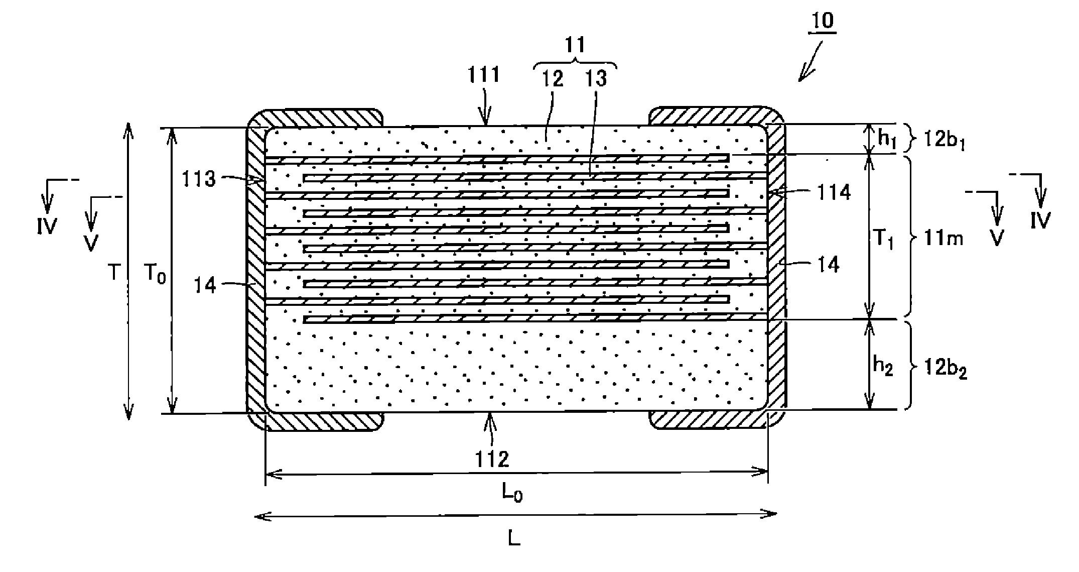
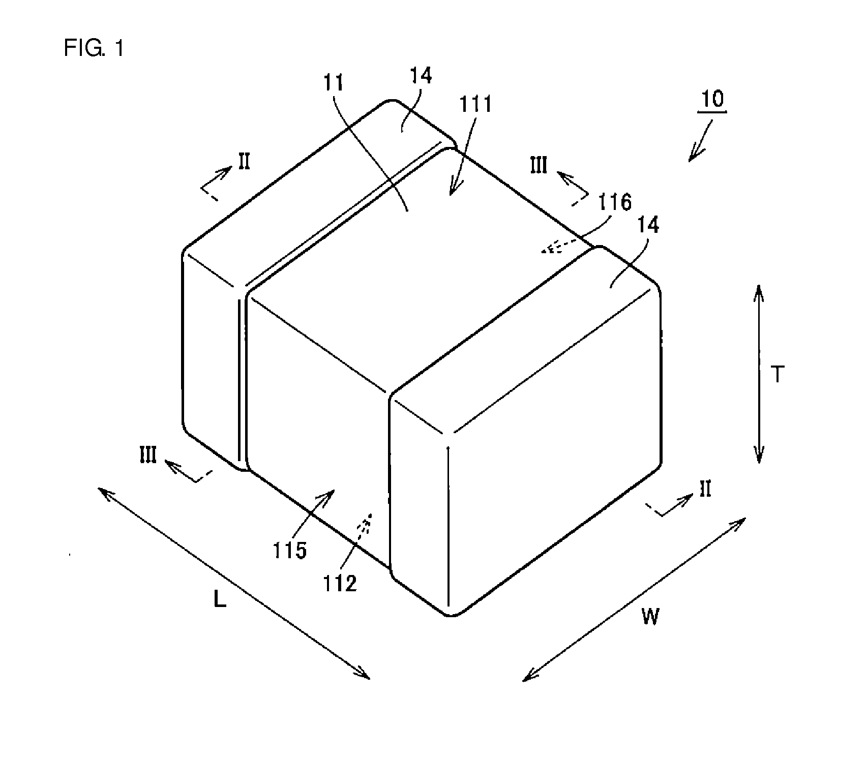
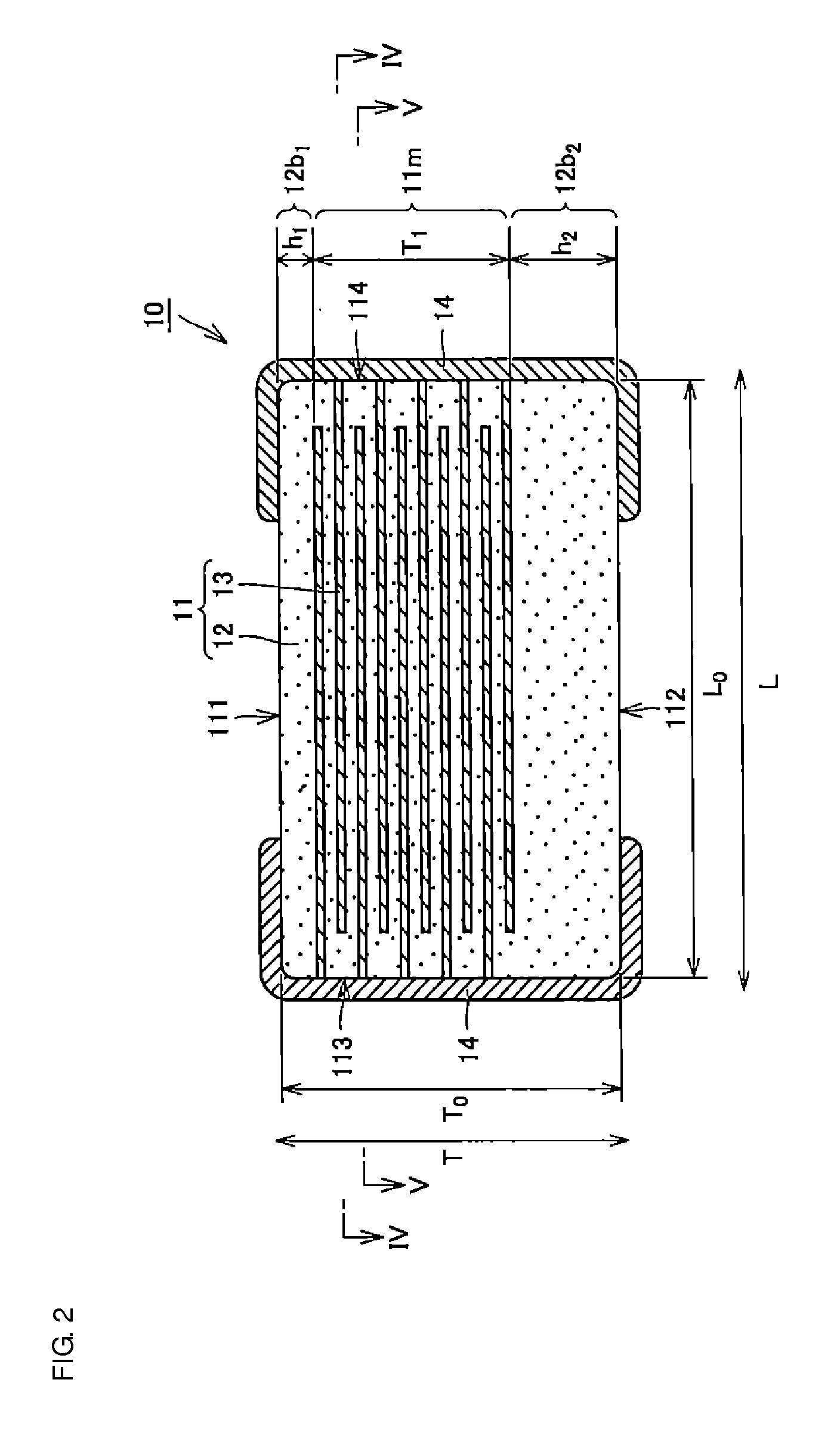
[0045]FIG. 1 is an external perspective view of a capacitor according to a first preferred embodiment of the present invention. FIGS. 2 and 3 are sectional views taken along lines II-II and III-III, respectively, of FIG. 1. FIGS. 4 and 5 are sectional views taken along lines IV-IV and V-V, respectively, of FIG. 2. In FIGS. 1 through 5, the length direction of a body 11, which will be discussed below, is indicated by L, the width direction thereof is indicated by W, and the height direction thereof is indicated by T.

[0046]As shown in FIGS. 1 through 5, the capacitor 10 includes the body 11 and two outer electrodes 14. The body 11 includes a plurality of dielectric layers 12 and a plurality of conductive layers 13 stacked on each other, and has first and second main surfaces 111 and 112 opposing each other in the stacking direction. The two outer electrodes 14 are disposed on some surfaces of the body 11 and are electrically connected to some of the plurality of conductive layers 13.

[...

second preferred embodiment

[0104]FIG. 10 is an external perspective view of a capacitor 10a according to the second preferred embodiment of the present invention. FIGS. 11 and 12 are sectional views taken along lines XI-XI and XII-XII, respectively, of FIG. 10. FIGS. 13 and 14 are sectional views taken along lines XIII-XIII and XIV-XIV, respectively, of FIG. 11. In FIGS. 10 through 14, the length direction of a body 11 is indicated by L, the width direction thereof is indicated by W, and the height direction thereof is indicated by T.

[0105]As shown in FIGS. 10 through 14, the capacitor 10a includes the body 11 and two outer electrodes 14. The body 11 includes a plurality of dielectric layers 12 and a plurality of conductive layers 13 stacked on each other, and includes first and second main surfaces 111 and 112 opposing each other in the stacking direction. The two outer electrodes 14 are disposed on some surfaces of the body 11 and are electrically connected to all the conductive layers 13.

[0106]The pluralit...

third preferred embodiment

[0179]The configuration of the boundary region of the outer portion 12b22 with the inner portion 12b21 of the body 11 of the capacitor is preferably implemented by a pressure-bonding method for a set of mother sheets. Accordingly, the pressure-bonding method for a set of mother sheets in the third preferred embodiment will first be described below.

[0180]FIG. 20 is a sectional view illustrating a state in which a set of mother sheets defining the capacitor in the third preferred embodiment are being pressure-bonded. The set of mother sheets shown in FIG. 20 is that as viewed from the same cross section as that shown in FIG. 17. In FIG. 20, the set of mother sheets corresponding to only two partial bodies 11p is shown.

[0181]As shown in FIG. 20, in the third preferred embodiment, a plurality of mother sheets defining the first outer layer portion 12b1, a plurality of mother sheets defining the inner layer portion 11m, and a plurality of mother sheets defining the inner portion 12b21 ar...


PUM

PropertyMeasurementUnit
heightaaaaaaaaaa
heightaaaaaaaaaa
heightaaaaaaaaaa

Abstract

A body of a multilayer ceramic capacitor includes an inner layer portion and first and second outer layer portions sandwiching the inner layer portion therebetween. The inner layer portion includes an area extending from a conductive layer positioned closest to a first main surface to a conductive layer positioned closest to a second main surface in the stacking direction. The height of the body is smaller than the width of the body. The height of the inner layer portion is smaller than the width of the inner layer portion. The first outer layer portion includes a dielectric layer positioned closest to the first main surface. The second outer layer portion includes a dielectric layer positioned closest to the second main surface, and is thicker than the first outer layer portion. The total height of the first and second outer layer portions is smaller than the height of the inner layer portion.

Description

BACKGROUND OF THE INVENTION[0001]1. Field of the Invention[0002]The present invention relates to a multilayer ceramic capacitor, a multilayer ceramic capacitor series including the same, and a multilayer ceramic capacitor mount body including the same.[0003]2. Description of the Related Art[0004]An example of the related art that discloses a multilayer ceramic capacitor in which the occurrence of cracks may be suppressed is Japanese Unexamined Patent Application Publication No. 2012-248581.[0005]In the multilayer ceramic capacitor disclosed in this publication, a base unit includes an inner electrode body (inner layer portion) and first and second dielectric bodies (outer layer portions). The inner electrode body includes first inner electrodes and second inner electrodes facing each other with a dielectric member therebetween and stacked on each other. The first and second dielectric bodies sandwich the inner electrode body therebetween in the stacking direction. The first dielectr...

Claims


Application Information

Patent Timeline
Patent Type & Authority Applications(United States)
IPC IPC(8): H01G4/30H01G4/012H01G4/12H01G4/224H01G4/38
CPCH01G4/30H01G4/38H01G4/224H01G4/12H01G4/012H01G4/1209
Inventor KITANO, SHOTAKATSUYAMA, TAKANOBUSUGITA, HIROAKI
Owner MURATA MFG CO LTD
Why Eureka
Try Eureka