Touch pixel design for reducing visual artifacts

a technology of touch pixel and visual artifact, which is applied in the field of touch sensor panels, can solve the problems of optical interference, touch screen visual artifacts, various visual artifacts, etc., and achieve the effect of reducing optical interference and reducing such visual artifacts

Inactive Publication Date: 2016-03-03
APPLE INC
View PDF6 Cites 12 Cited by
  • Summary
  • Abstract
  • Description
  • Claims
  • Application Information

AI Technical Summary

Benefits of technology

[0004]Some capacitive touch sensor panels can be formed by a matrix of substantially transparent conductive plates made of materials such as Indium Tin Oxide (ITO), and some touch screens can be formed by partially integrating touch sensing circuitry into a display pixel stackup (i.e., the stacked material layers forming the display pixels). The layout of the transparent conductive plates (e.g., touch pixels, or touch electrodes) on the touch screen can cause certain visual artifacts to appear on the touch screen. For example, regions outside of the touch pixels can have different ITO coverage than regions inside the touch pixels. Further, the edges of touch pixels can cause optical interference with the edges of display pixels that may exist in a layer of the touch screen that is below the touch pixels. These layout characteristics can cause various visual artifacts on the touch screen. The examples of the disclosure provide various techniques for reducing such visual artifacts. In some examples, the ITO coverage in different regions of the touch screen is substantially equalized. In some examples, the edges of touch pixels and other features on the touch screen are designed to be non-linear to reduce optical interference with display pixels that may exist below the touch pixels.

Problems solved by technology

The layout of the transparent conductive plates (e.g., touch pixels, or touch electrodes) on the touch screen can cause certain visual artifacts to appear on the touch screen.
Further, the edges of touch pixels can cause optical interference with the edges of display pixels that may exist in a layer of the touch screen that is below the touch pixels.
These layout characteristics can cause various visual artifacts on the touch screen.

Method used


Image

  • Touch pixel design for reducing visual artifacts
  • Touch pixel design for reducing visual artifacts
  • Touch pixel design for reducing visual artifacts

Examples


Embodiment Construction

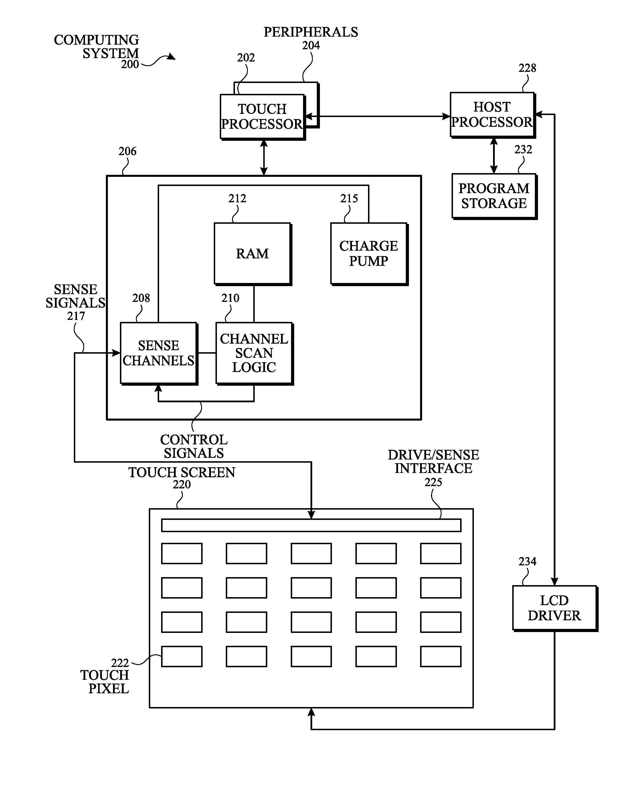
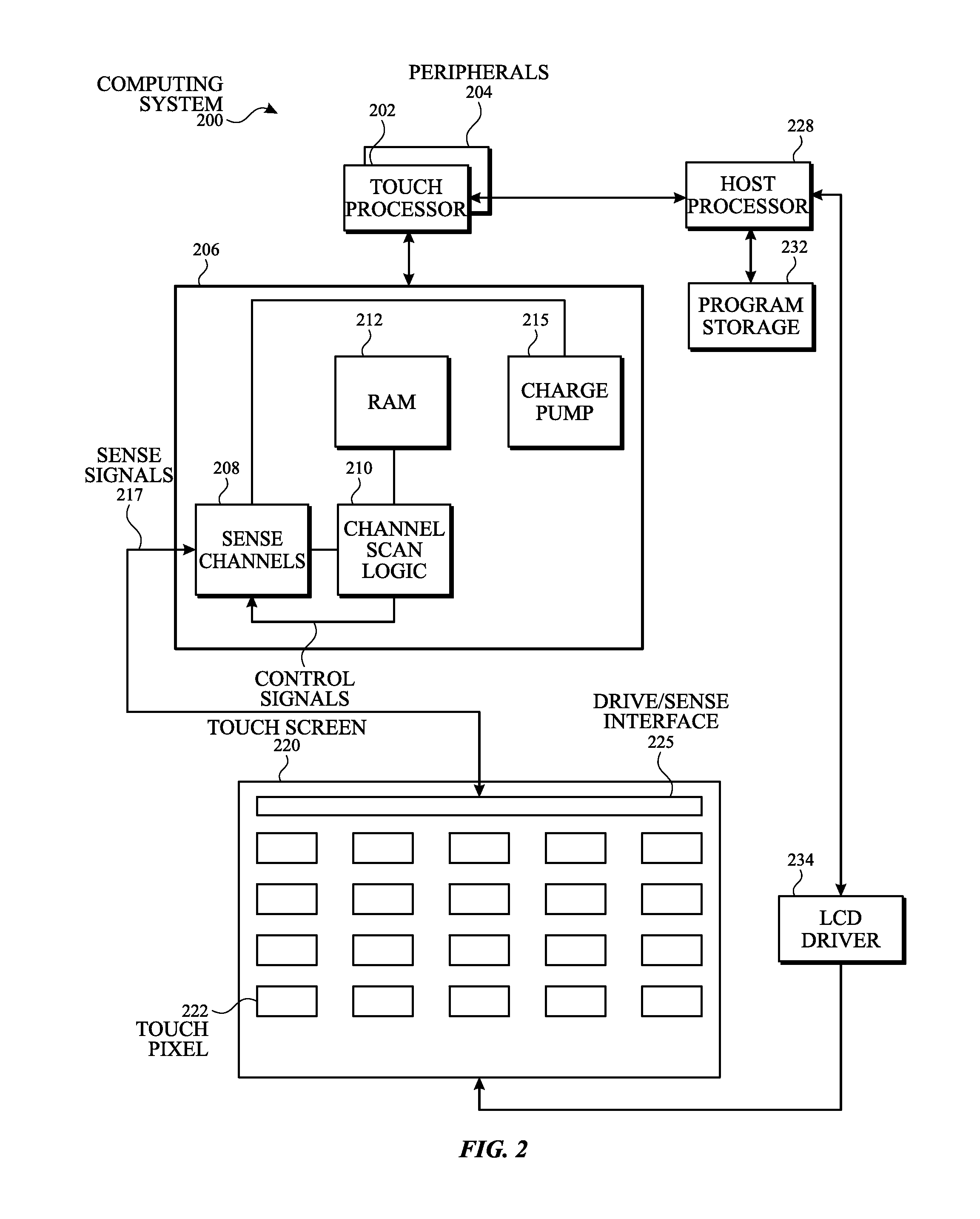
[0016]In the following description of examples, reference is made to the accompanying drawings which form a part hereof, and in which it is shown by way of illustration specific examples that can be practiced. It is to be understood that other examples can be used and structural changes can be made without departing from the scope of the disclosed examples.

[0017]Some capacitive touch sensor panels can be formed by a matrix of substantially transparent conductive plates made of materials such as Indium Tin Oxide (ITO), and some touch screens can be formed by partially integrating touch sensing circuitry into a display pixel stackup (i.e., the stacked material layers forming the display pixels). The layout of the transparent conductive plates (e.g., touch pixels, or touch electrodes) on the touch screen can cause certain visual artifacts to appear on the touch screen. For example, regions outside of the touch pixels can have different ITO coverage than regions inside the touch pixels....


PUM


Abstract

A touch sensor panel is disclosed. In some examples, the touch sensor panel comprises a first touch pixel electrode formed in a first layer, the first touch pixel electrode comprising a plurality of electrically coupled touch pixel segments separated by one or more touch pixel gaps. In some examples, the touch sensor panel comprises a sense connection formed in the first layer and coupled to the first touch pixel electrode, the sense connection configured to couple the first touch pixel electrode to sense circuitry. In some examples, the touch pixel segments and the touch pixel gaps are configured to provide optical uniformity on the touch sensor panel.

Description

FIELD OF THE DISCLOSURE[0001]This relates generally to touch sensor panels, and more particularly to touch pixel designs for reducing visual artifacts on a touch screen.BACKGROUND OF THE DISCLOSURE[0002]Many types of input devices are presently available for performing operations in a computing system, such as buttons or keys, mice, trackballs, joysticks, touch sensor panels, touch screens and the like. Touch screens, in particular, are becoming increasingly popular because of their ease and versatility of operation as well as their declining price. Touch screens can include a touch sensor panel, which can be a clear panel with a touch-sensitive surface, and a display device such as a liquid crystal display (LCD) that can be positioned partially or fully behind the panel so that the touch-sensitive surface can cover at least a portion of the viewable area of the display device. Touch screens can allow a user to perform various functions by touching the touch sensor panel using a fin...

Claims


Application Information

Patent Timeline
Patent Type & Authority Applications(United States)
IPC IPC(8): G06F3/044
CPCG06F2203/04103G06F3/044G06F2203/04112G06F3/041G06F3/0412G06F3/04164G06F3/0443G06F3/0448G06F3/0446
Inventor PEDDER, JAMES, EDWARD, ALEXANDERSHIH, DAVID, H.C.GRUNTHANER, MARTIN, PAULHOTELLING, STEVEN, P.
Owner APPLE INC
Why Eureka
Try Eureka